Methods And Systems For Characterization Of An X-Ray Beam With High Spatial Resolution

a technology of spatial resolution and characterization method, applied in the field of x-ray metrology system and methods, can solve the problems of difficult optical radiation penetration to the bottom layer, difficult characterization, and increased difficulty in characterization, and achieve the effect of easy determination

Active Publication Date: 2018-11-15
KLA TENCOR TECH CORP
View PDF5 Cites 17 Cited by
  • Summary
  • Abstract
  • Description
  • Claims
  • Application Information

AI Technical Summary

Benefits of technology

[0024]In another aspect, a SAXS metrology system employs at least one beam occlusion calibration target to locate an x-ray illumination beam with respect to the specimen positioning system. The beam occlusion calibration target includes at least one marker and a cylindrically shaped occlusion element. An alignment camera is employed to locate the marker in coordinates of the specimen positioning system. The location of the marker with respect to the cylindrically shaped occlusion element is known apriori (e.g., with an accuracy of less than 200 nanometers). Thus, the location of the cylindrically shaped occlusion element in coordinates of the specimen positio

Problems solved by technology

As devices (e.g., logic and memory devices) move toward smaller nanometer-scale dimensions, characterization becomes more difficult.
Devices incorporating complex three-dimensional geometry and materials with diverse physical properties contribute to characterization difficulty.
For example, modern memory structures are often high-aspect ratio, three-dimensional structures that make it difficult for optical radiation to penetrate to the bottom layers.
Optical metrology tools utilizing infrared to visible light can penetrate many layers of translucent materials, but longer wavelengths that provide good depth of penetration do not provide sufficient sensitivity to small anomalies.
As a result, the parameters characterizing the target often cannot be reliably decoupled with available measurements.
However, the mirror like structure of 3D FLASH intrinsically causes decreasing light intensity as the illumination propagates deeper into the film stack.
This causes sensitivity loss and correlation issues at depth.
In this scenario, SCD is only able to successfully extract a reduced set of metrology dimensions with high sensitivity and low correlation.
Optical radiation is often unable to penetrate layers constructed of these materials.
As a result, measurements with thin-film scatterometry tools such as ellipsometers or reflectometers are becoming increasingly challenging.
However, these approaches have not reliably overcome fundamental challenges associated with measurement of many advanced targets (e.g., complex 3D structures, structures smaller than 10 nm, structures employing opaque materials) and measurement applications (e.g., line edge roughness and line width roughness measurements).
Atomic force microscopes (AFM) and scanning-tunneling microscopes (STM) are able to achieve atomic resolution, but they can only probe the surface of the specimen.
In addition, AFM and STM microscopes require long scanning times. Scanning electron microscopes (SEM) achieve intermediate resolution levels, but are unable to penetrate structures to sufficient depth.
Thus, high-aspect ratio holes are not characterized well.
In addition, the required charging of the specimen has an adverse effect on imaging performance.
X-ray reflectometers

Method used


Image

  • Methods And Systems For Characterization Of An X-Ray Beam With High Spatial Resolution
  • Methods And Systems For Characterization Of An X-Ray Beam With High Spatial Resolution
  • Methods And Systems For Characterization Of An X-Ray Beam With High Spatial Resolution

Examples


Embodiment Construction

[0056]Reference will now be made in detail to background examples and some embodiments of the invention, examples of which are illustrated in the accompanying drawings.

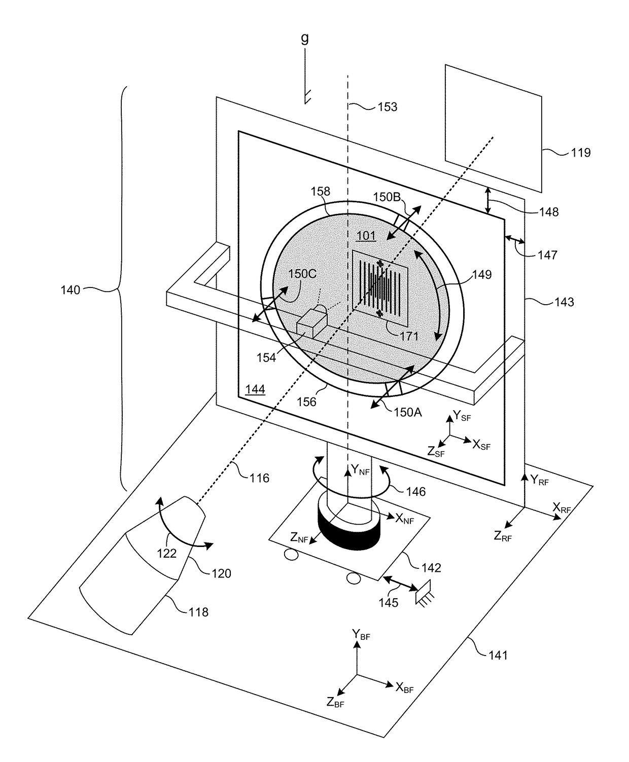
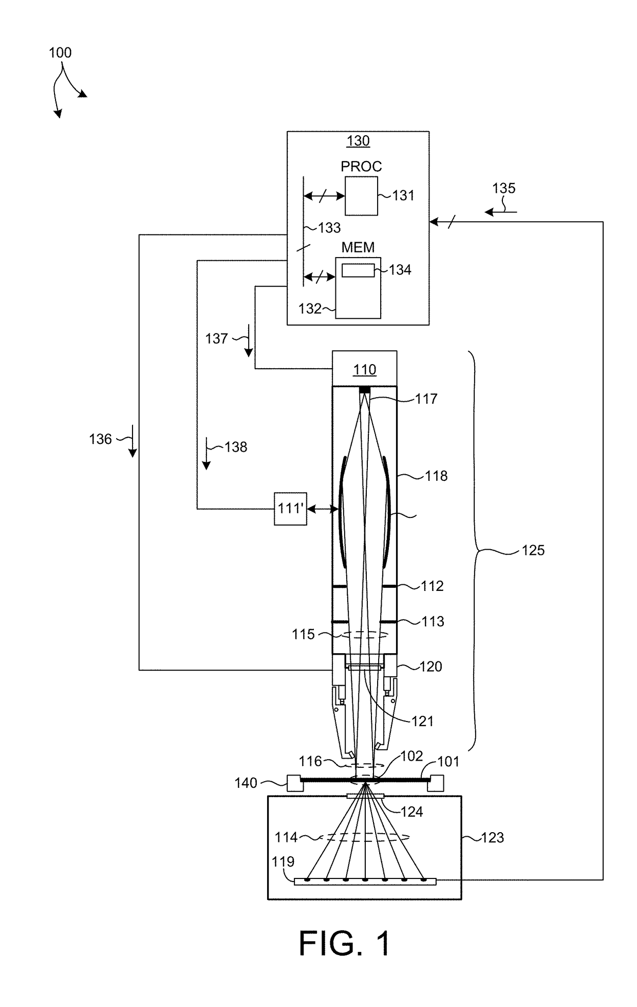
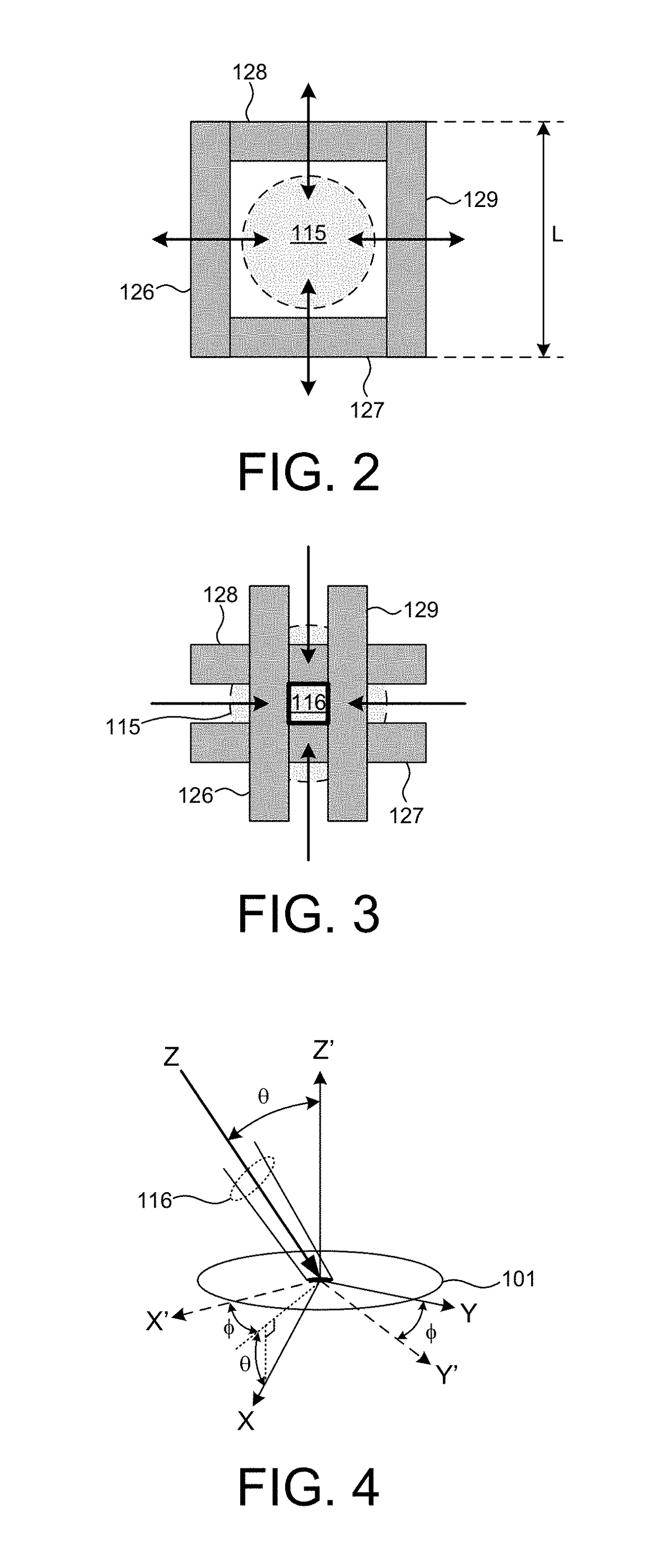
[0057]Methods and systems for positioning a specimen and characterizing an x-ray beam incident onto the specimen in a Transmission, Small-Angle X-ray Scatterometry (T-SAXS) metrology system are described herein. Practical T-SAXS measurements in a semiconductor manufacturing environment require measurements over a large range of angles of incidence and azimuth with respect to the surface of a specimen (e.g., semiconductor wafer) with a small beam spot size (e.g., less than 50 micrometers across the effective illumination spot). Accurate positioning of the wafer and characterization of the beam size and shape are required to achieve small measurement box size. In addition, calibrations that accurately locate the illumination beam on the desired target area on the surface of a semiconductor wafer over the full range of i...


PUM


Abstract

Methods and systems for positioning a specimen and characterizing an x-ray beam incident onto the specimen in a Transmission, Small-Angle X-ray Scatterometry (T-SAXS) metrology system are described herein. A specimen positioning system locates a wafer vertically and actively positions the wafer in six degrees of freedom with respect to the x-ray illumination beam without attenuating the transmitted radiation. In some embodiments, a cylindrically shaped occlusion element is scanned across the illumination beam while the detected intensity of the transmitted flux is measured to precisely locate the beam center. In some other embodiments, a periodic calibration target is employed to precisely locate the beam center. The periodic calibration target includes one or more spatially defined zones having different periodic structures that diffract X-ray illumination light into distinct, measurable diffraction patterns.

Description

CROSS REFERENCE TO RELATED APPLICATION[0001]The present application for patent claims priority under 35 U.S.C. § 119 from U.S. provisional patent application Ser. No. 62 / 505,014, filed May 11, 2017, the subject matter of which is incorporated herein by reference in its entirety.TECHNICAL FIELD[0002]The described embodiments relate to x-ray metrology systems and methods, and more particularly to methods and systems for improved measurement accuracy.BACKGROUND INFORMATION[0003]Semiconductor devices such as logic and memory devices are typically fabricated by a sequence of processing steps applied to a specimen. The various features and multiple structural levels of the semiconductor devices are formed by these processing steps. For example, lithography among others is one semiconductor fabrication process that involves generating a pattern on a semiconductor wafer. Additional examples of semiconductor fabrication processes include, but are not limited to, chemical-mechanical polishing...

Claims


Application Information

Patent Timeline
IPC IPC(8): G01N23/201H01L21/67G01N23/205H01L21/68G01N23/207H01L21/687
CPCG01N23/201H01L21/67282G01N23/205H01L21/681G01N2223/6116H01L21/67288H01L21/67259H01L21/68764G01N23/207G01N23/223G01N23/2204H01L22/00
Inventor BYKANOV, ALEXANDERARTEMIEV, NIKOLAYDI REGOLO, JOSEPH A.GELLINEAU, ANTONIOKUZNETSOV, ALEXANDERVELDMAN, ANDREIHENCH, JOHN
Owner KLA TENCOR TECH CORP
Why Eureka
Try Eureka