Touch Panel and Trace Structure Thereof

a technology of trace structure and touch panel, which is applied in the direction of printed circuits, instruments, computing, etc., can solve the problems of low yield rate, high cost, and drawbacks of the fabrication process of metal oxide films

Active Publication Date: 2018-11-22
TPK GLASS SOLUTIONS XIAMEN
View PDF5 Cites 13 Cited by
  • Summary
  • Abstract
  • Description
  • Claims
  • Application Information

AI Technical Summary

Benefits of technology

[0005]In some embodiments of the present disclosure, the metal traces are designed to be covered by the covers which are at least formed of metal nanowires, thereby achieving the protection effect on the metal traces. For example, the exposed surfaces of the metal traces are protected in the process of forming the touch sensing electrodes by etching the conductive film layer containing the metal nanowires. In addition, in some embodiments of the present disclosure, novel methods for forming the touch electrodes and the traces thereof are proposed, and therefore structures of the touch panels are different from traditional touch panels.

Problems solved by technology

However, the fabrication process of the metal oxide films may have drawbacks such as high cost, complicated process, and low yield rate.
In some situations, patterned metal oxide electrodes are readily visible to user which is a drawback as well.
However, issues persist regarding fabrication processes using the nanowires.

Method used


Image

  • Touch Panel and Trace Structure Thereof
  • Touch Panel and Trace Structure Thereof
  • Touch Panel and Trace Structure Thereof

Examples


Embodiment Construction

[0038]Reference will now be made in detail to the present embodiments of the disclosure, examples of which are illustrated in the accompanying drawings. Wherever possible, the same reference numbers are used in the drawings and the description to refer to the same or like parts.

[0039]As used herein, “around”, “about” or “approximately” shall generally mean within 20 percent, preferably within 10 percent, and more preferably within 5 percent of a given value or range. Numerical quantities given herein are approximate, meaning that the term “around”, “about” or “approximately” can be inferred if not expressly stated. In addition, as used herein, “film layer”, “coating layer,”“polymer,” or “precursor” shall mean identical or similar elements, the difference therebetween mainly lying in the curing state thereof, and it is noted the terms may be alternatively used below for convenience of illustration.

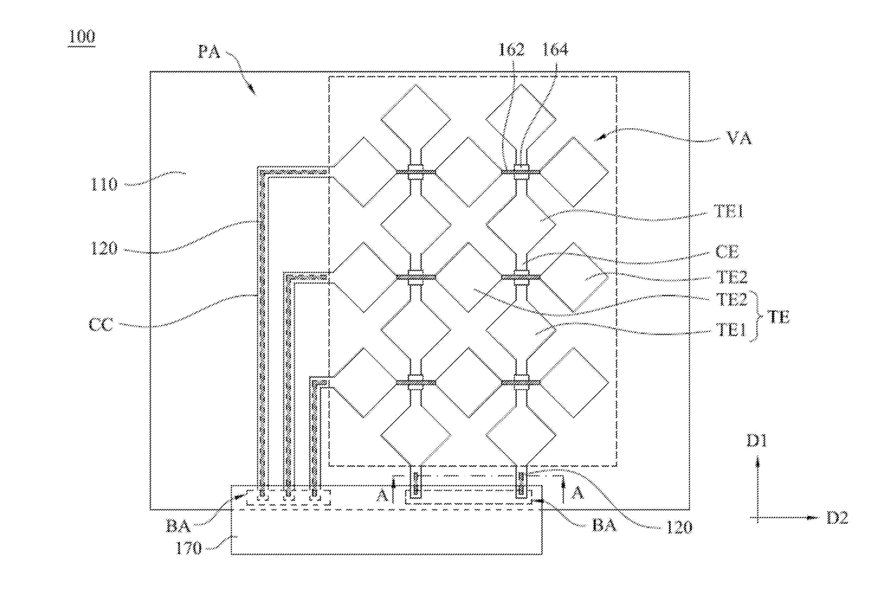
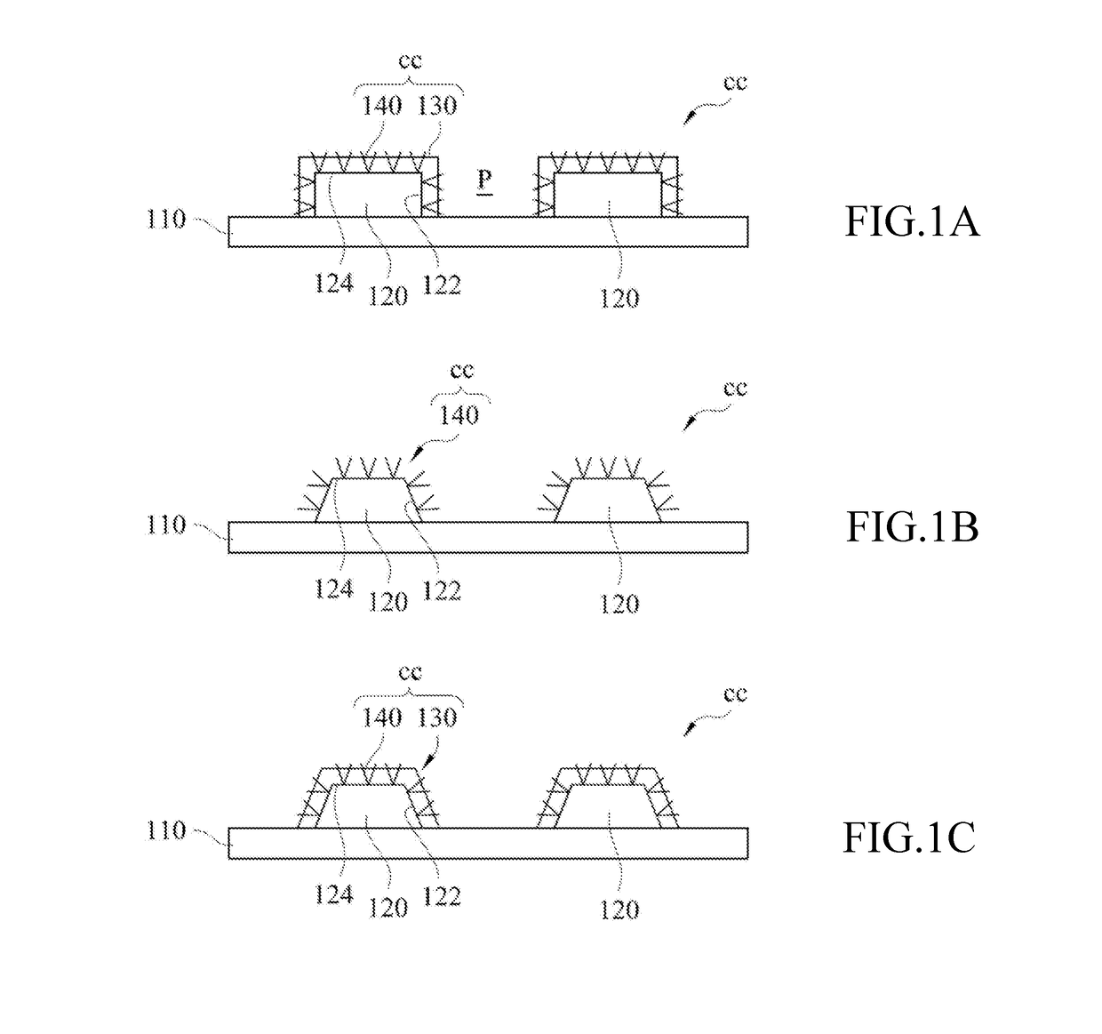
[0040]FIG. 1 is a schematic top view of a touch panel 100 according to some embodiments...


PUM

PropertyMeasurementUnit
diameteraaaaaaaaaa
diameteraaaaaaaaaa
diameteraaaaaaaaaa

Abstract

A trace structure includes a substrate, at least one metal trace, and a cover. The metal trace is disposed on the substrate, and has sidewalls and a top surface. The cover is disposed on the sidewalls and the top surface of the metal trace, and the cover includes metal nanowires. The cover and the metal trace have different etch resistances.

Description

CROSS-REFERENCE TO RELATED APPLICATION[0001]This application claims priority to China Application Serial Number 201710387754.0, filed May 22, 2017, which is herein incorporated by reference.BACKGROUNDTechnical Field[0002]The present disclosure relates to touch panels and trace structures thereof.Description of Related Art[0003]In recent years, transparent conductors, which are capable of transmitting light and providing suitable conductivity, are widely used in various display or touch devices. In general, transparent conductors may be various metal oxides, such as indium tin oxide (ITO), indium zinc oxide (IZO), cadmium tin oxide (CTO), or aluminum-doped zinc oxide (AZO). The metal oxide films may be formed by physical vapor deposition or chemical vapor deposition process, and patterned by photolithography. However, the fabrication process of the metal oxide films may have drawbacks such as high cost, complicated process, and low yield rate. In some situations, patterned metal oxid...

Claims


Application Information

Patent Timeline
Patent Type & Authority Applications(United States)
IPC IPC(8): G06F3/047G06F3/041H05K1/18
CPCG06F3/047G06F3/0412H05K1/189G06F2203/04103G06F3/0416G06F3/044G06F2203/04112G06F2203/04111H05K1/097H05K2201/026H05K2201/0391G06F3/04164G06F3/0446G06F3/0443G06F3/0445G06F3/0448
Inventor LI, JUI-HSINGLEE, LIEN-HSIN
Owner TPK GLASS SOLUTIONS XIAMEN
Why Eureka
Try Eureka