
Method of manufacturing semiconductor devices and corresponding product

Active Publication Date: 2018-11-29
STMICROELECTRONICS SRL
View PDF3 Cites 22 Cited by
  • Summary
  • Abstract
  • Description
  • Claims
  • Application Information

AI Technical Summary

Benefits of technology

The patent describes a method for creating flexible and efficient electronic components. The method involves using a special type of metal lead frame that allows for better power dissipation and vibration resistance, making it suitable for use in automotive products. The lead frame is designed with a certain degree of down setting, which helps to fill in the areas around the lead with a molding compound, allowing for the creation of internal traces and routings. This method also allows for the creation of BGA-like traces on a QFP package, which makes it easier to assemble complex devices by keeping the external factor of the package simple. Overall, the patent provides a way to create highly flexible and efficient electronic components using a special metal lead frame and advanced molding techniques.

Problems solved by technology

Providing wire bonding in semiconductor devices or packages, such as integrated circuits of the QFP (Quad Flat Pack) or the QFN (Quad Flat No-lead) type, may turn out to be a critical issue (e.g., due to lead distance being unfeasible by stamping at lead tip), especially in the presence of a high number of input / output lines.

Method used


Image

  • Method of manufacturing semiconductor devices and corresponding product
  • Method of manufacturing semiconductor devices and corresponding product
  • Method of manufacturing semiconductor devices and corresponding product

Examples


Embodiment Construction

[0043]In the ensuing description, one or more specific details are illustrated, aimed at providing an in-depth understanding of examples of embodiments of this description. The embodiments may be obtained without one or more of the specific details, or with other methods, components, materials, etc. In other cases, known structures, materials, or operations are not illustrated or described in detail so that certain aspects of embodiments will not be obscured.

[0044]Reference to “an embodiment” or “one embodiment” in the framework of the present description is intended to indicate that a particular configuration, structure, or characteristic described in relation to the embodiment is comprised in at least one embodiment. Hence, phrases such as “in an embodiment” or “in one embodiment” that may be present in one or more points of the present description do not necessarily refer to one and the same embodiment. Moreover, particular conformations, structures, or characteristics may be com...


PUM


Abstract

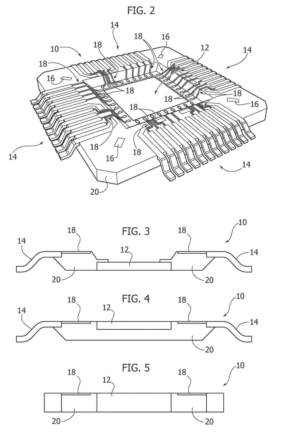
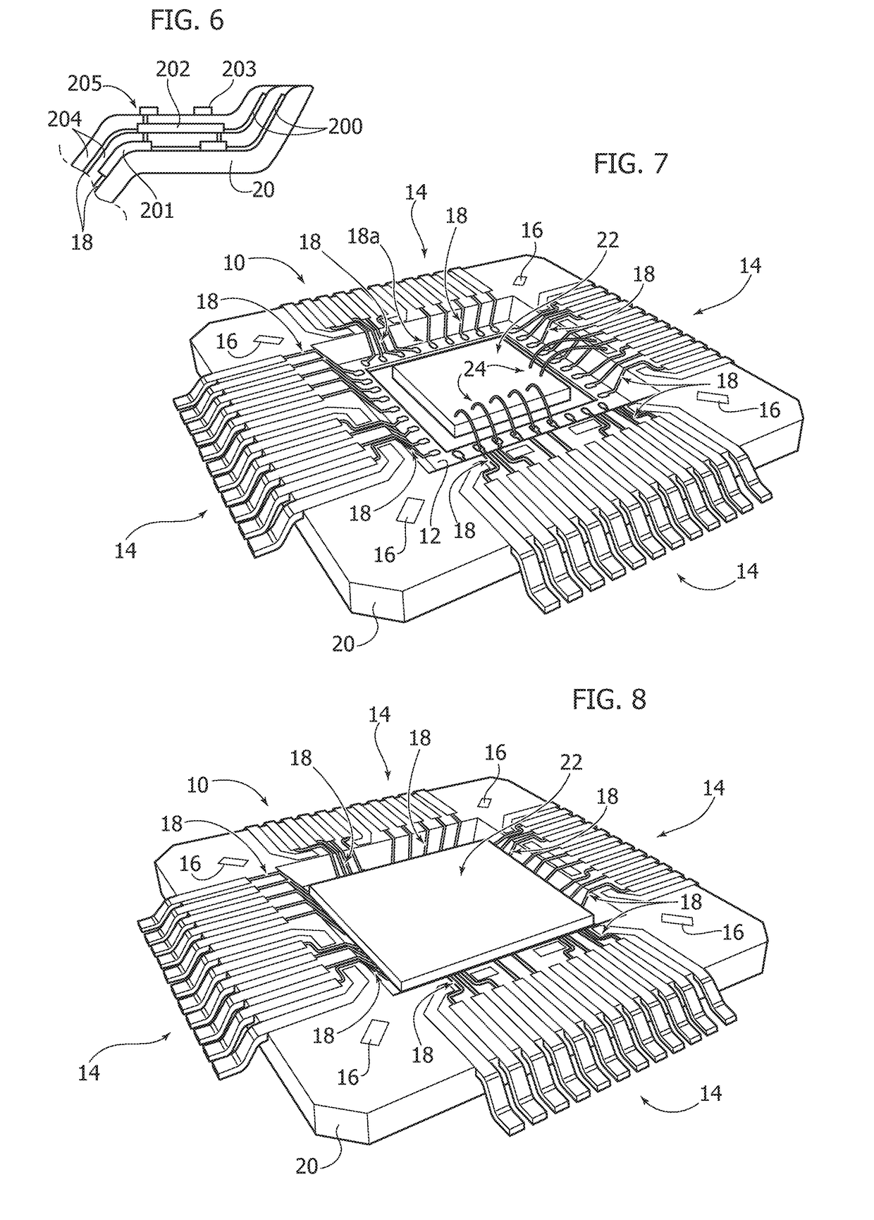
A method of manufacturing semiconductor products includes: providing a semiconductor product lead frame including a semiconductor die mounting area and an array of electrically conductive leads, molding semiconductor product package molding material, e.g., laser direct structuring material, and forming on the package molding material molded onto the lead frame electrically-conductive lines extending between the semiconductor die mounting area and the array of electrically-conductive leads.

Description

BACKGROUNDTechnical Field[0001]The description relates to semiconductor devices, such as, e.g., integrated circuits (IC).Description of the Related Art[0002]Providing wire bonding in semiconductor devices or packages, such as integrated circuits of the QFP (Quad Flat Pack) or the QFN (Quad Flat No-lead) type, may turn out to be a critical issue (e.g., due to lead distance being unfeasible by stamping at lead tip), especially in the presence of a high number of input / output lines.[0003]Wire length being too long for certain wires, wire looping and wire proximity represent possible additional factors to be taken into account.[0004]Advanced QFP technology may resort to hybrid solutions by adopting routing and bonding concepts as derived from BGA (Ball Grid Array) technology. Such arrangements may include passive components, such as capacitors.[0005]Various papers presented at the 12th International Congress On Molded Interconnect Devices (MID) held at WUrzburg, Germany on 28-29 Sep. 20...

Claims


Application Information

Patent Timeline
IPC IPC(8): H01L23/498H01L21/56H01L21/48H01L23/00H01L23/31H01L25/10H01L25/00
CPCH01L23/49861H01L21/565H01L21/486H01L24/85H01L23/3121H01L23/49838H01L2224/48245H01L25/105H01L23/49827H01L25/50H01L2224/48091H01L2224/48101H01L24/48H01L21/4867H01L23/3107H01L23/13H01L23/49541H01L23/49548H01L2224/32245H01L2224/48247H01L2224/73265H01L2224/24175H01L2224/16245H01L2224/73253H01L2224/32145H01L2924/19107H01L2924/15192H01L2924/19105H01L2924/19041H01L2924/15153H01L24/24H01L24/16H01L24/32H01L2224/49173H01L24/73H01L2224/82103H01L2924/00012H01L2924/00
Inventor ZIGLIOLI, FEDERICO GIOVANNI
Owner STMICROELECTRONICS SRL
Learn More