Configurable molecular switch array

a molecular switch and array technology, applied in multi-programming arrangements, instruments, pulse techniques, etc., can solve the problem of minimal signal degradation and the implementation of complex logical functions

Inactive Publication Date: 2004-03-04
HEWLETT PACKARD DEV CO LP
View PDF14 Cites 51 Cited by
  • Summary
  • Abstract
  • Description
  • Claims
  • Application Information

AI Technical Summary

Benefits of technology

0028] FIG. 15 is a schematic diagram of a configurable molecular switch array similar to FIG. 11, depicting the formation of a diode by joining a p-type vertical wire with the n-type horizontal wire in the right lower quadrant that does not interfere with the correct functioning of the gates configured in the array because of the "push-pull" nature of the configured field effect transistors.

Problems solved by technology

Thus, rather complex logical functions can be implemented with minimal signal degradation.

Method used


Image

  • Configurable molecular switch array
  • Configurable molecular switch array
  • Configurable molecular switch array

Examples


Embodiment Construction

[0029] Definitions

[0030] As used herein, the term "reconfigurable" means that a switch can change its state multiple times via a reversible process such as an oxidation or reduction; in other words, the switch can be opened and closed multiple times such as the memory bits in a random access memory.

[0031] The term "bi-stable" as applied to a molecule means a molecule having two relatively low energy states. The molecule may be either irreversibly switched from one state to the other (singly configurable) or reversibly switched from one state to the other (reconfigurable).

[0032] The term "micron-scale dimensions" refers to dimensions that range from 1 micrometer to a few micrometers in size.

[0033] The term "sub-micron scale dimensions" refers to dimensions that range from 1 micrometer down to 0.04 micrometers.

[0034] The term "nanometer scale dimensions" refers to dimensions that range from 0.1 nanometers to 50 nanometers (0.05 micrometers).

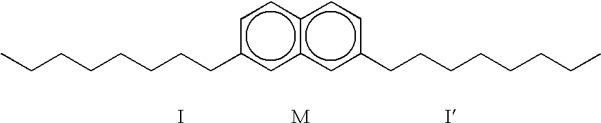
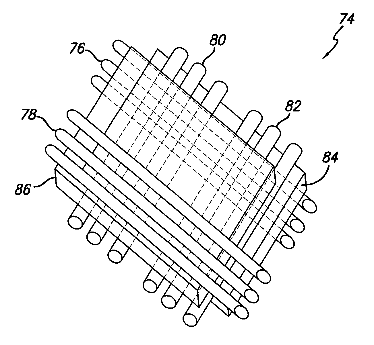
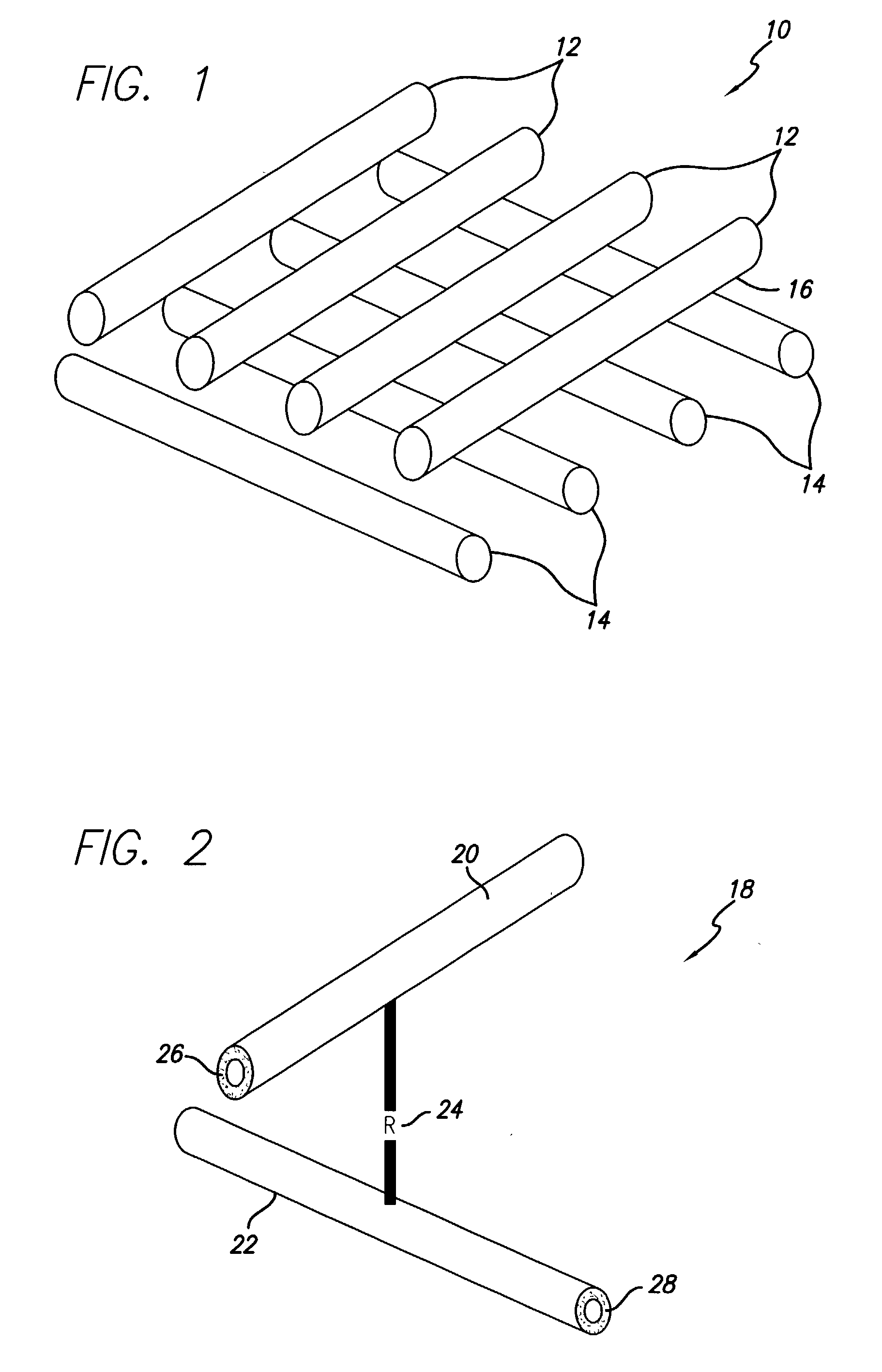
[0035] A crossbar is an array of switches th...


PUM


Abstract

A computing system for implementing at least one electronic circuit with gain comprises at least one two-dimensional molecular switch array. The molecular switch array is formed by assembling two or more crossed planes of wires into a configuration of devices. Each device comprises a junction formed by a pair of crossed wires and at least one connector species that connects the pair of crossed wires in the junction. The junction has a functional dimension in nanometers, and includes a switching capability provided by both (1) one or more connector species and the pair of crossed wires and (2) a configurable nano-scale wire transistor having a first state that functions as a transistor and a second state that functions as a conducting semiconductor wire. Specific connections are made to interconnect the devices and connect the devices to two structures that provide high and low voltages.

Description

[0001] The present invention relates generally to electronic devices whose functional length scales are measured in nanometers, and, more particularly, to configurable molecular switch arrays based on crossed nanometer-scale wires joined by bi-stable molecular scale switches at the intersecting junctions.[0002] The silicon integrated circuit and its continued miniaturization has created an electronics industry that is now facing its limit due to economic and physical constraints. Current integrated circuit devices are being manufactured using sub-micron scale dimensions, while new solutions are enabling the development of nanometer scale devices.[0003] Prior proposed solutions to the problem of constructing nanometer scale devices have involved (1) the utilization of extremely fine scale lithography using X-rays, electrons, ions, scanning probes, or stamping to define the device components; (2) direct writing of the device components by electrons, ions, or scanning probes; or (3) th...

Claims


Application Information

Patent Timeline
Patent Type & Authority Applications(United States)
IPC IPC(8): G06F9/50G11C13/02H01L21/82H01L27/10H01L27/28H01L51/05H03K17/00H01L29/06
CPCB82Y10/00G11C13/0009G11C13/0014H01L27/285G11C2213/34G11C2213/77G11C2213/81G11C2213/14H10K19/202G06F15/78H01L27/12
Inventor SNIDER, GREGORY S.KUEKES, PHILIP J.WILLIAMS, R. STANLEY
Owner HEWLETT PACKARD DEV CO LP
Why Eureka
Try Eureka