Eureka AIR delivers breakthrough ideas for toughest innovation challenges, trusted by R&D personnel around the world.

Method and system for implementing byte-alterable write cache

Active Publication Date: 2018-12-06
ALIBABA GRP HLDG LTD
View PDF4 Cites 13 Cited by
  • Summary
  • Abstract
  • Description
  • Claims
  • Application Information

AI Technical Summary

Benefits of technology

This patent describes a data storage system that includes a communication interface for receiving write commands from a host and two write caches. The first write cache stores data before sending it to a high-capacity storage device, while the second write cache receives data from the first and updates its content. The first write cache uses a command-processing unit to determine which parts of data need to be updated and sends a page mask to a media controller to facilitate the update. The system also includes a transfer buffer for simultaneously transferring data to the high-capacity storage device. The technical effects include improved performance and efficiency in data storage and retrieval.

Problems solved by technology

Because magnetic-based hard disk drives (HDD) are often too slow to handle high-frequency writes, current computer systems often implement a Not AND (NAND gate-based solid-state drive (SSD) as a write cache, which can collect write commands and cache them until the hard disk can be written to later.
However, handling high-frequency small random writes can still be a challenge to NAND SSDs.
Hence, changing a single byte in a page will require the entire page to be rewritten and, thus, can lead to high write amplification and significantly faster wearing of the drive.
Moreover, NAND SSDs cannot be updated in-place; instead, pages must be erased before they can be written.
Changing a single byte in a page can cause the whole page to be invalidated and redirected to a new page.
Consequently, high-frequency small writes can cause an SSD to run out of clean page quickly, triggering expensive garbage-collection operations.
This can lead to a severely degraded performance.

Method used


Image

  • Method and system for implementing byte-alterable write cache
  • Method and system for implementing byte-alterable write cache
  • Method and system for implementing byte-alterable write cache

Examples


Embodiment Construction

[0023]The following description is presented to enable any person skilled in the art to make and use the embodiments, and is provided in the context of a particular application and its requirements. Various modifications to the disclosed embodiments will be readily apparent to those skilled in the art, and the general principles defined herein may be applied to other embodiments and applications without departing from the spirit and scope of the present disclosure. Thus, the present invention is not limited to the embodiments shown, but is to be accorded the widest scope consistent with the principles and features disclosed herein.

Overview

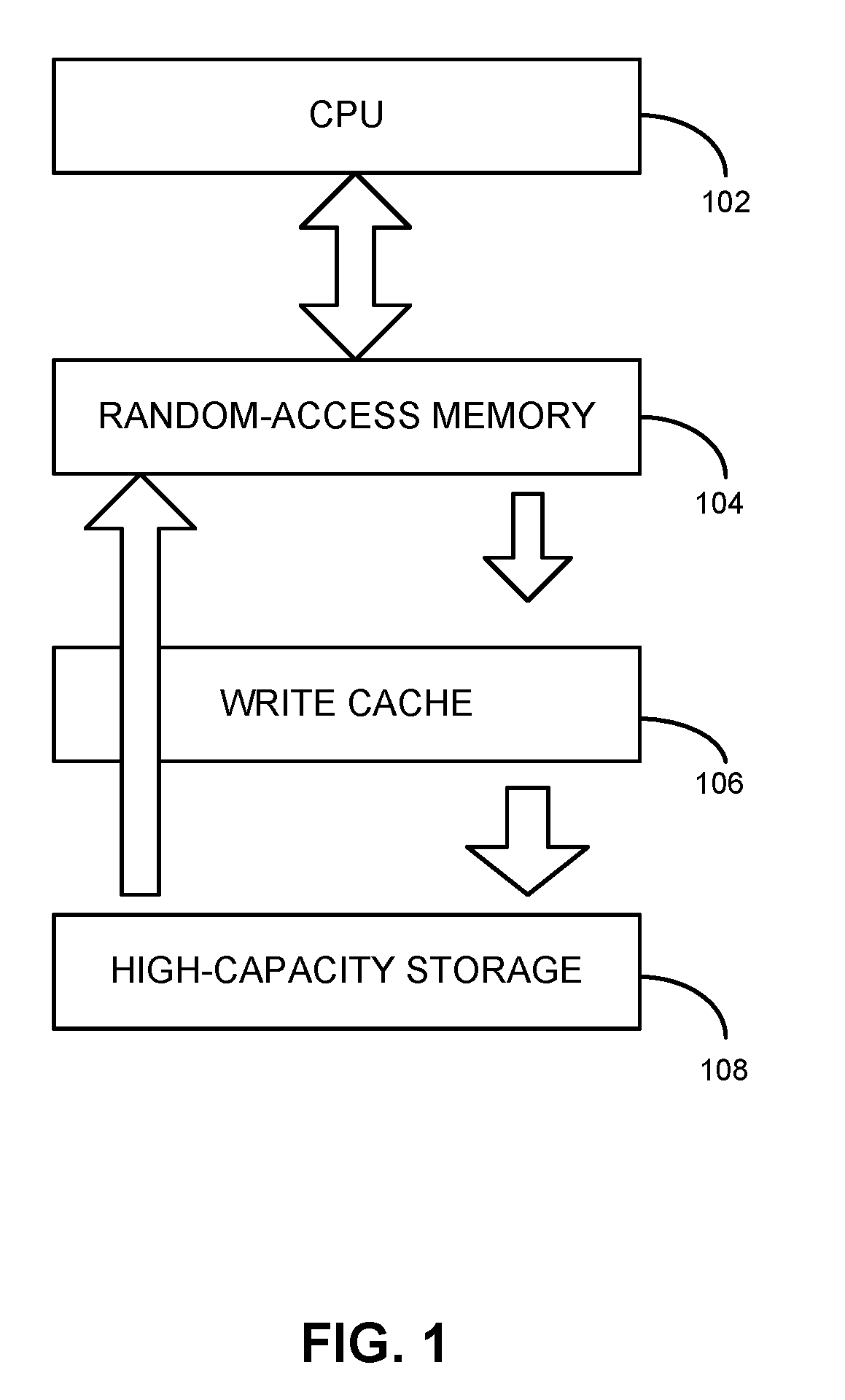
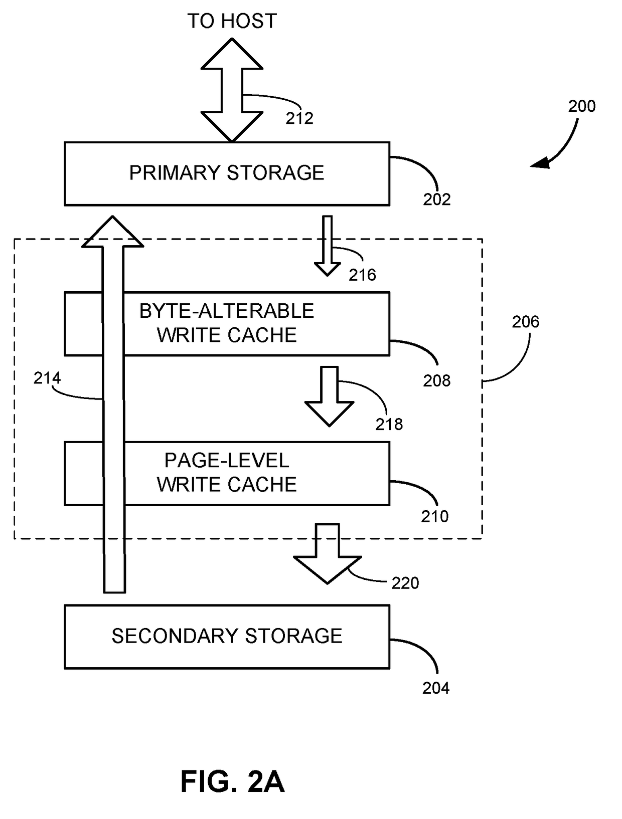
[0024]Embodiments of the present invention solve the problem of improving efficiency and reducing hardware wear associated with high-frequency write operations by facilitating a novel byte-alterable write cache. More specifically, the byte-alterable write cache can be based on Storage Class Memory (SCM), which can provide much higher endurance, low...


PUM


Abstract

One embodiment described herein provides a data storage system. The storage system includes a communication interface for receiving a write command from a host of the data storage system and a first write cache coupled to the host via the communication interface. The write command includes to-be-written data and address information associated with the to-be-written data. The first write cache is configured to temporarily store the to-be-written data before sending the to-be-written data to a high-capacity storage device coupled to the host, and the first write cache is configured to update its content by performing byte-level in-place writing based on the received write command.

Description

BACKGROUNDField[0001]This disclosure is generally related to data storage devices and systems. More specifically, this disclosure is related to a data storage system that implements a write cache that allows high-frequency write operations.Related Art[0002]Data storage devices play an important role in modern computing, especially in eras of cloud computing and big data. Many of the enterprise or high-performance computational workloads (e.g., key-value databases, data analytics, transactional databases) exhibit a high ratio of small random writes at runtime.[0003]Because magnetic-based hard disk drives (HDD) are often too slow to handle high-frequency writes, current computer systems often implement a Not AND (NAND gate-based solid-state drive (SSD) as a write cache, which can collect write commands and cache them until the hard disk can be written to later. Alternatively, the HDD may be replaced by the faster NAND SSD. However, handling high-frequency small random writes can still...

Claims


Application Information

Patent Timeline
IPC IPC(8): G06F3/06G06F12/0804G06F12/0893
CPCG06F3/0619G06F12/0804G06F12/0893G06F3/0685G06F3/0656G06F3/0659G06F3/064G06F12/0868G06F12/0888G06F12/0897G06F2212/1021G06F2212/1024G06F2212/1032G06F2212/313
Inventor ZHOU, PINGLI, SHU
Owner ALIBABA GRP HLDG LTD
Why Eureka
Eureka Blog
Learn More