

System and method for key parameter identification, process model calibration and variability analysis in a virtual semiconductor device fabrication environment
a technology of key parameters and process models, applied in the field of system and method for key parameter identification, process model calibration and variability analysis in a virtual semiconductor device fabrication environment, can solve the problems of increasing the complexity of integrated semiconductor fabrication processes, long experimental runs, and negative or null characterization
- Summary
- Abstract
- Description
- Claims
- Application Information
AI Technical Summary
Benefits of technology
Problems solved by technology
Method used
Image

Examples
Embodiment Construction
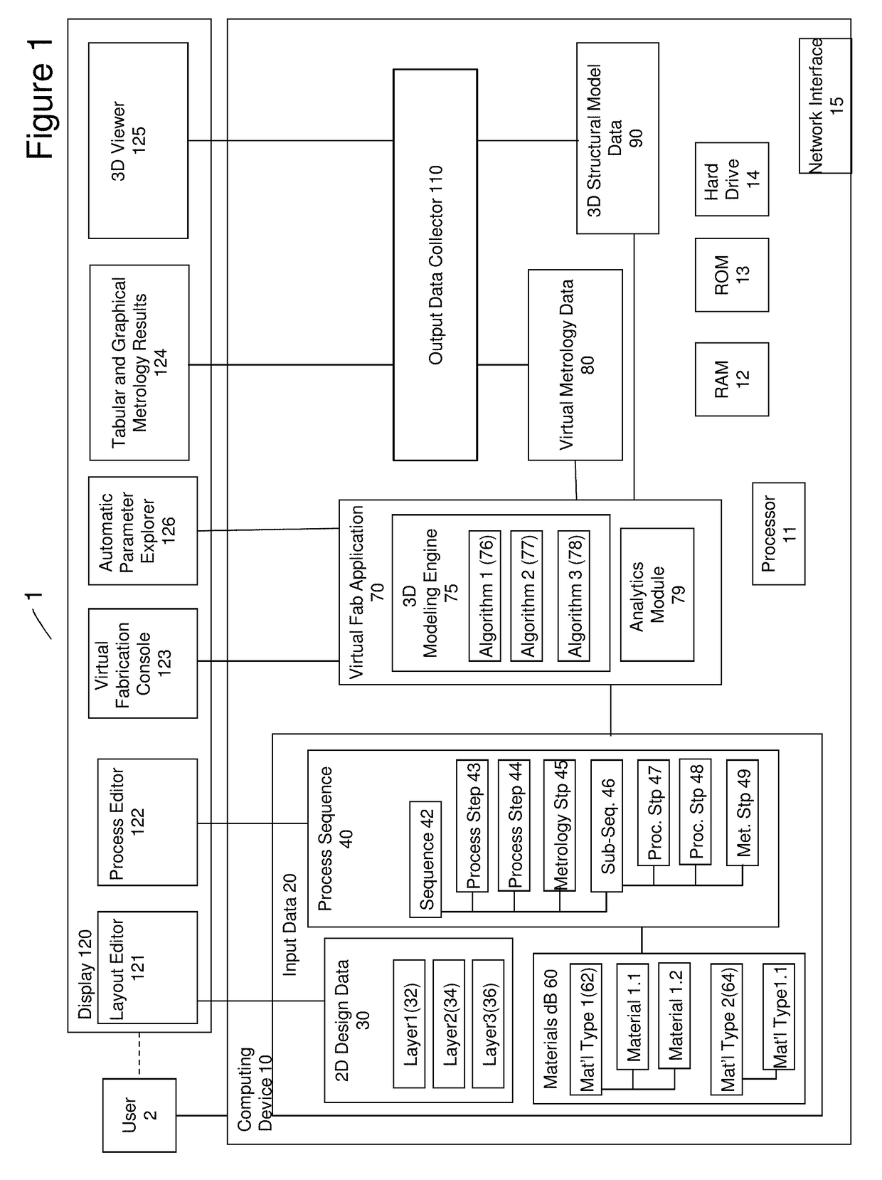
[0034]Embodiments of the present invention provide a virtual fabrication environment for semiconductor device fabrication that includes an analytics module for identifying key parameters and for performing process model calibration and variability analysis. However, prior to discussing the key parameter identification, process model calibration, optimization, variability analysis and other features provided by embodiments, an exemplary 3D design environment / virtual fabrication environment into which an analytics module of the present invention may be integrated is first described.
Exemplary Virtual Fabrication Environment
[0035]FIG. 1 depicts an exemplary virtual fabrication environment 1 suitable for practicing an embodiment of the present invention. Virtual fabrication environment 1 includes a computing device 10 accessed by a user 2. Computing device 10 is in communication with a display 120. Display 120 may be a display screen that is part of computing device 10 or may be a separa...
PUM
 Abstract
Description
Claims
Application Information