A detector device with majority current and a circuitry for controlling the current

a detector device and circuitry technology, applied in the field of detector devices, can solve the problems of high readout noise and reading time, and achieve the effect of overcoming the problem of reading noise and high readout nois

Active Publication Date: 2019-01-24
SONY DEPTHSENSING SOLUTIONS SA NV
View PDF0 Cites 6 Cited by
  • Summary
  • Abstract
  • Description
  • Claims
  • Application Information

AI Technical Summary

Benefits of technology

[0009]The pixel detector device of the present invention can comprise control circuitry arranged for controlling the first source and controlling individually at least one of said first majority carrier currents. Thanks to this individual control, one larger pixel is artificially created and the operational pixel structure is enlarged to a bigger virtual pixel zone, similar to what would happen if the data of the pixels were binned together during post-processing. This individual control offers the advantage of requiring only one read-out for the artificially bigger pixel. Thanks to the individual control, both issues of reading time and high readout noise are overcome.

Problems solved by technology

A challenge in Time-of-Flight sensors based on CAPD pixel devices is to optimize the TOF sensor and system to the needs of the encountered use cases and situations.

Method used


Image

  • A detector device with majority current and a circuitry for controlling the current
  • A detector device with majority current and a circuitry for controlling the current
  • A detector device with majority current and a circuitry for controlling the current

Examples


Embodiment Construction

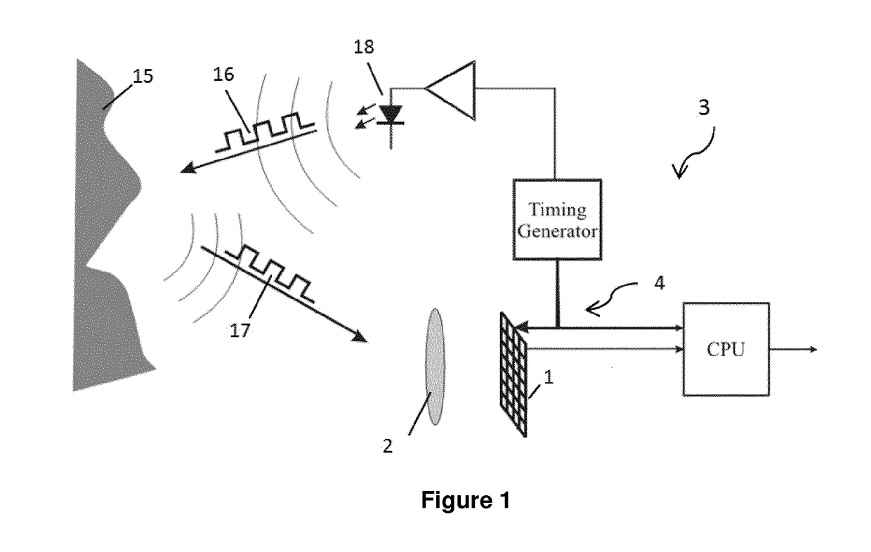
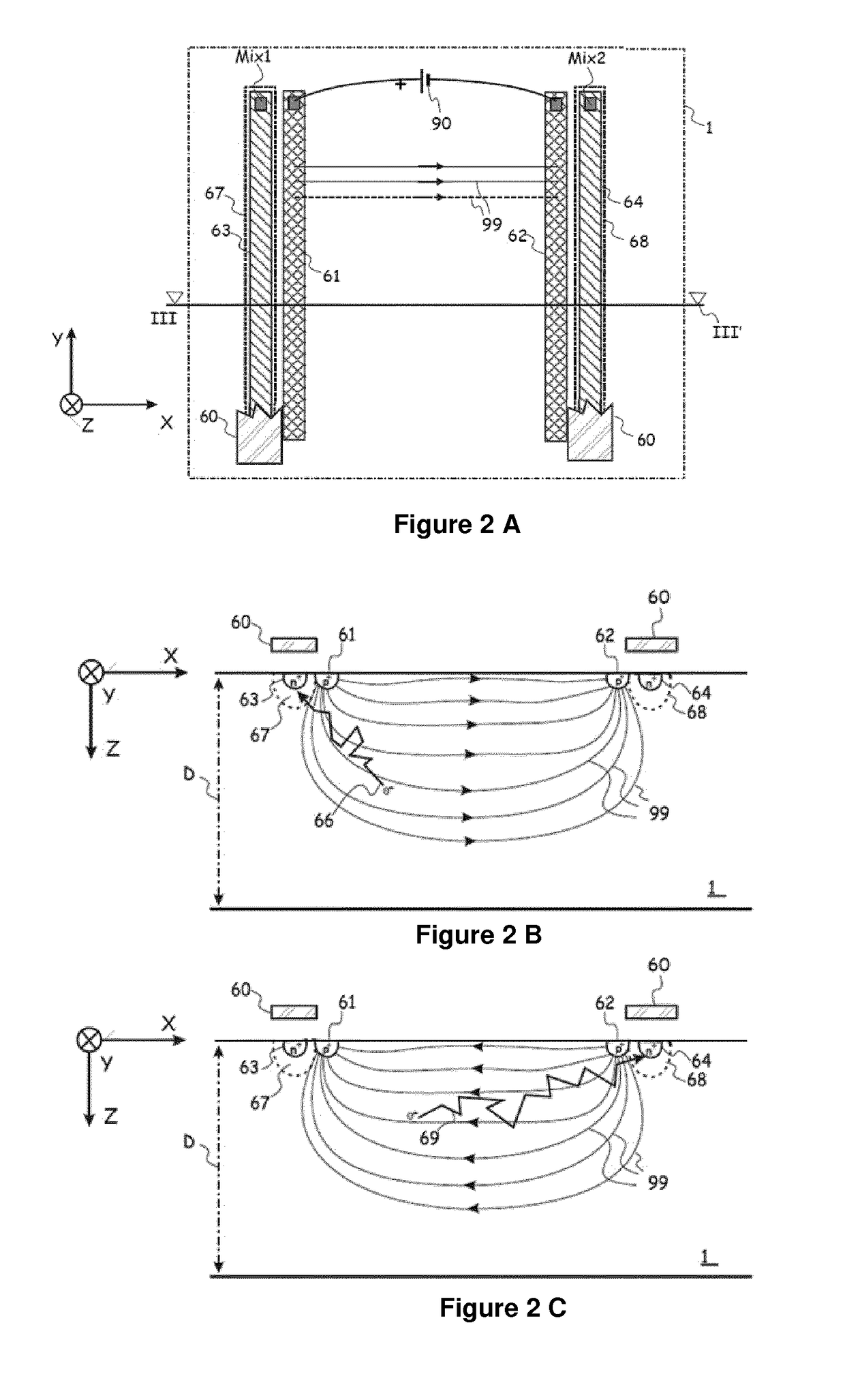
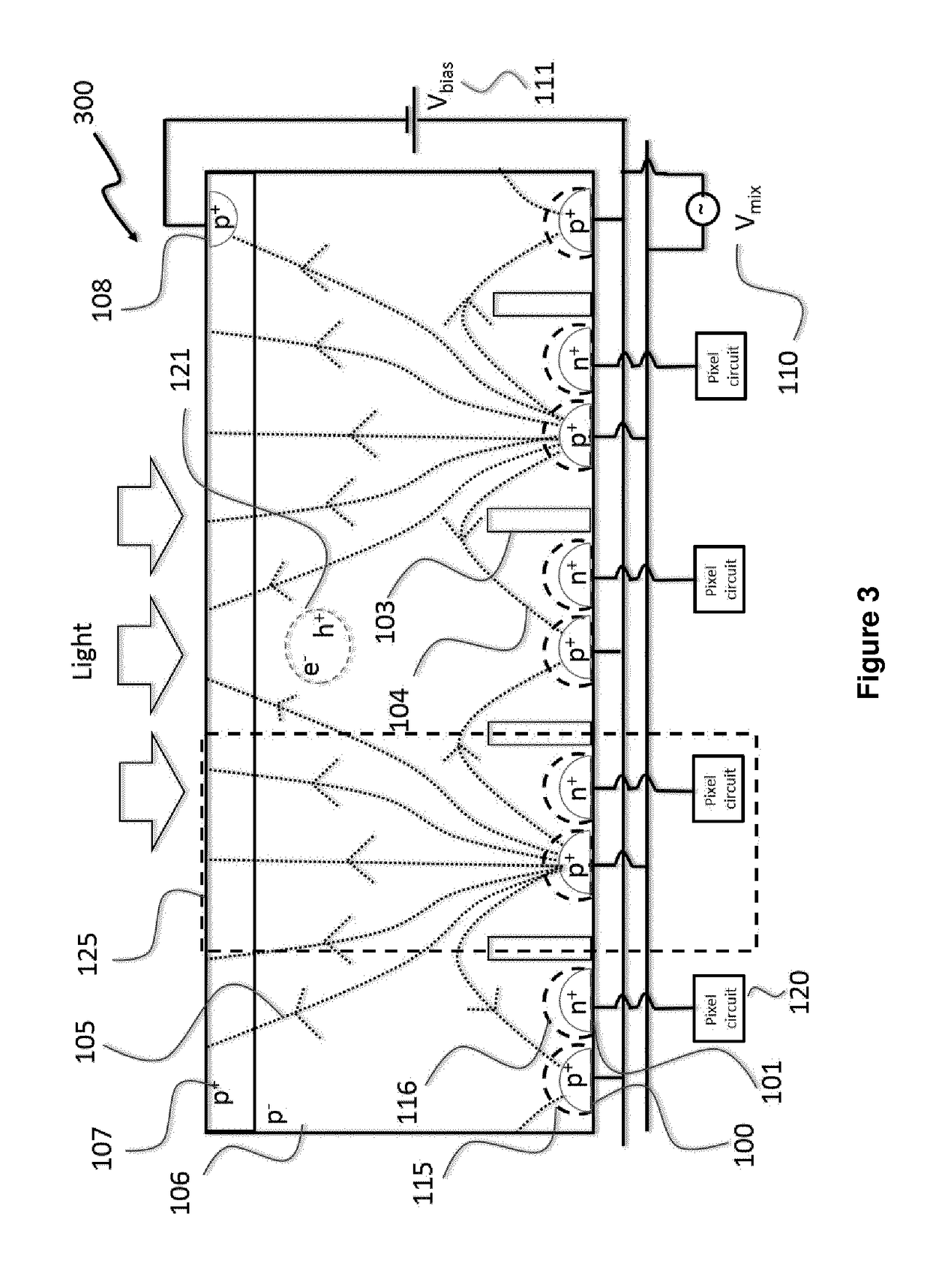
[0023]The present invention will be disclosed in reference to a detection device 300 also termed SENSOR. The detection device 300 contains PIXELS 125 also referred as PIXEL. Typically the Pixel 125 contains at least 1 TAP, consisting of at least 1 detection region and at least 1 control region also referred as TAP.

[0024]The invention will also be explained with reference to p-type epitaxial layer and substrate, but the present invention includes within its scope a complementary device whereby p and n regions become n and p regions respectively. A skilled person can make such modification without departing from the spirit of the invention.

[0025]It should also be understood that the terms n, p, n+, p+ and p−, n-well, p-well, deep n-well and deep p-well are well known by the one skilled in the art. The terms n, p, n+, p+ and p− refer to ranges of doping levels in semiconductor materials well known by the one skilled in the art.

[0026]The terms n and p refer to n-doped and p-doped region...


PUM


Abstract

The invention relates to a detector device assisted by majority current, comprising a semiconductor layer of a first conductivity type, a plurality of control regions of the first conductivity type, at least one detection region of a second conductivity type opposite to the first conductivity type and a first source for generating a majority carrier current associated with an electrical field, characterized in that it further comprises control circuitry arranged for controlling the first source and controlling individually at least one of said first majority carrier currents.

Description

TECHNICAL FIELD OF THE INVENTION[0001]The invention relates to a detector device assisted by majority current for detecting an electromagnetic radiation impinging on a semiconductor layer, wherein a majority carrier current is generated between two control regions and wherein photo-generated minority carriers are directed towards a detection region under the influence of an electrical field generated between the control regions.[0002]The invention can be used in imagers, particularly Time-Of-Flight imagers.BACKGROUND OF THE INVENTION[0003]Nowadays, more and more detection devices implement Time-Of-Flight (TOF) technologies for obtaining depth information. A basic Time-Of-Flight (TOF) camera system 3 is illustrated in FIG. 1. TOF camera systems capture 3D images of a scene 15 by analysing the time of flight of light from a light source 18 to an object. TOF camera system 3 includes a camera with a dedicated illumination unit 18 and data processing means 4.[0004]The operational princip...

Claims


Application Information

Patent Timeline
Patent Type & Authority Applications(United States)
IPC IPC(8): G01S7/486H01L27/146G01S17/36H04N5/341G01S17/89G01S7/4863G01S17/894
CPCG01S7/4863H01L27/1461G01S17/36H04N5/341G01S17/89G01S7/493H01L27/1464G05F1/10H01L27/14609G01S17/894H04N25/40
Inventor VAN DER TEMPEL, WARDVAN NIEUWENHOVE, DANIEL
Owner SONY DEPTHSENSING SOLUTIONS SA NV
Why Eureka
Try Eureka