Detector device with majority current and a circuitry for controlling the current

a technology of circuitry and current, applied in the direction of radio frequency controlled devices, television systems, instruments, etc., to overcome the problems of reading time and high readout nois

Active Publication Date: 2022-01-11
SONY DEPTHSENSING SOLUTIONS SA NV
View PDF32 Cites 1 Cited by
  • Summary
  • Abstract
  • Description
  • Claims
  • Application Information

AI Technical Summary

Benefits of technology

[0010]In prior art the optical area of each single pixel in a sensor is allocated to the N taps (or detection regions) of the pixel. Control regions (p-implants in the case of CAPD devices, polysilicon gates in the case of PMD devices, etc) allow the taps to collect intermittently the minority carriers generated in the optical area during the active window of each tap. In case the pixel is built with only one tap, a dump or drain node is foreseen in the pixel to dump the minority carriers generated in the time-window outside of the active window of the tap. This is the prior art conventional TOF pixel architecture in which each pixel is an in theory closed system if non-idealities such as blooming and crosstalk are not considered.The present invention introduces the concept of collaborative pixels, where each pixel is operating together with surrounding pixels. The principle applies mainly to TOF pixels consisting of a single tap but can be expanded to more taps per pixel.Each pixel now may share at least one part or portion of its optical area, said optical area being also termed volume, with surrounding pixels and likewise the surrounding pixels may share at least one part or portion of their optical area with at least the optical area of at least another pixel. The control region of the pixel controls the activity window of the detection region (or tap). In the ON state the detection region gathers minority carriers generated in its optical area but also gathers from surrounding shared optical areas of pixels in inactive or OFF state. In the OFF state the optical area becomes available for the gathering of minority carriers by the nearest active neighbours.By careful control of the individual tap control signals the pattern created by the collaborative pixels in the sensor can be adjusted. Also, using the right control signal pixel could become completely inactive (for example with Not Connected control signal) and bypassed in the collaboration. This allows adjustment of the actual resolution of the sensor as the complete image sensor area is now distributed over fewer operational taps. Such a careful control not only enables creating overlapping virtual pixel zones (200) by sharing one or more portions of the associated volume of a pixel with one or more neighbouring pixels, but it further enables the change of the optical
[0011]The pixel detector device of the present invention can comprise control circuitry arranged for controlling the first source and controlling individually at least one of said first majority carrier currents. Thanks to this individual control, one larger pixel is artificially created and the operational pixel structure is enlarged to a bigger virtual pixel zone, similar to what would happen if the data of the pixels were binned together during post-processing. This individual control offers the advantage of requiring only one read-out for the artificially bigger pixel. Thanks to the individual control, both issues of reading time and high readout noise are overcome.

Problems solved by technology

A challenge in Time-of-Flight sensors based on CAPD pixel devices is to optimize the TOF sensor and system to the needs of the encountered use cases and situations.

Method used


Image

  • Detector device with majority current and a circuitry for controlling the current
  • Detector device with majority current and a circuitry for controlling the current
  • Detector device with majority current and a circuitry for controlling the current

Examples


Embodiment Construction

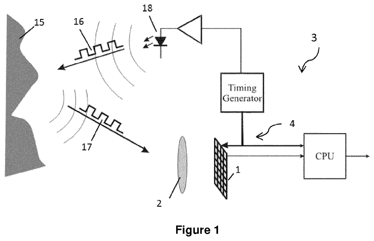
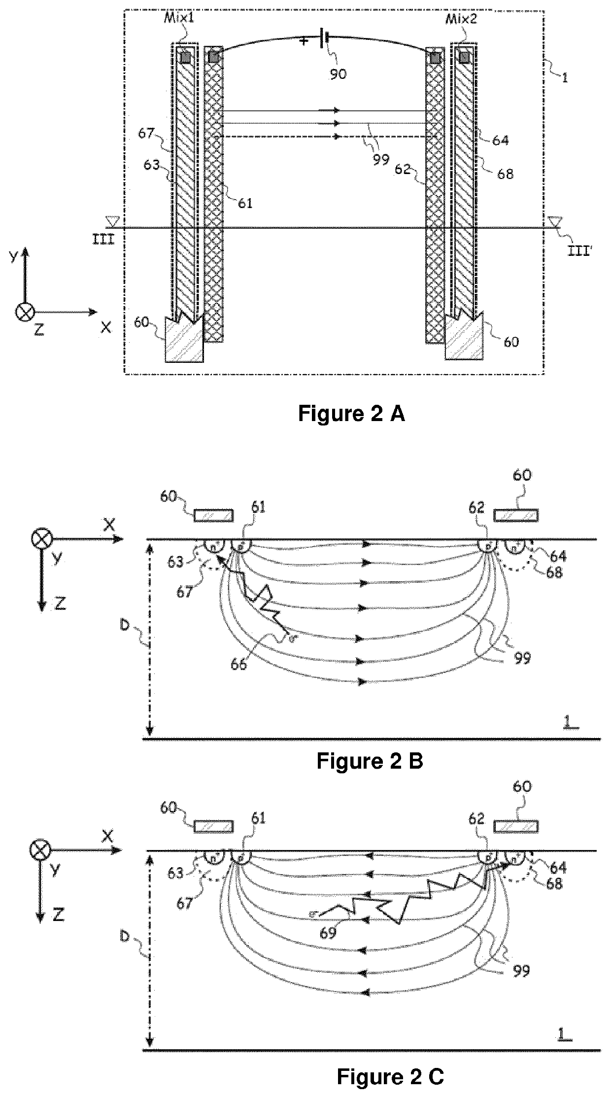
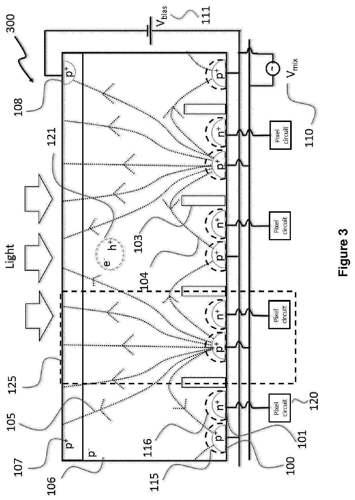
[0025]The present invention will be disclosed in reference to a detection device 300 also termed SENSOR. The detection device 300 contains PIXELS 125 also referred as PIXEL. Typically the Pixel 125 contains at least 1 TAP, consisting of at least 1 detection region and at least 1 control region also referred as TAP.

[0026]The invention will also be explained with reference to p-type epitaxial layer and substrate, but the present invention includes within its scope a complementary device whereby p and n regions become n and p regions respectively. A skilled person can make such modification without departing from the spirit of the invention.

[0027]It should also be understood that the terms n, p, n+, p+ and p−, n-well, p-well, deep n-well and deep p-well are well known by the one skilled in the art. The terms n, p, n+, p+ and p− refer to ranges of doping levels in semiconductor materials well known by the one skilled in the art.

[0028]The terms n and p refer to n-doped and p-doped region...


PUM

PropertyMeasurementUnit
conductivityaaaaaaaaaa
conductivity typeaaaaaaaaaa
electrical fieldaaaaaaaaaa

Abstract

The invention relates to a detector device assisted by majority current, comprising a semiconductor layer of a first conductivity type, a plurality of control regions of the first conductivity type, at least one detection region of a second conductivity type opposite to the first conductivity type and a first source for generating a majority carrier current associated with an electrical field, characterized in that it further comprises control circuitry arranged for controlling the first source and controlling individually at least one of said first majority carrier currents.

Description

[0001]This Application is a national stage filing under 35 U.S.C. 371 of International Patent Application Serial No. PCT / EP2017 / 050602, filed Jan. 12, 2017, entitled “A DETECTOR DEVICE WITH MAJORITY CURRENT AND A CIRCUITRY FOR CONTROLLING THE CURRENT”. Foreign priority benefits are claimed under 35 U.S.C. § 119(a)-(d) or 35 U.S.C. § 365(b) of European application number 16151588.7, filed Jan. 15, 2016. The entire contents of these applications are incorporated herein by reference in their entirety.TECHNICAL FIELD OF THE INVENTION[0002]The invention relates to a detector device assisted by majority current for detecting an electromagnetic radiation impinging on a semiconductor layer, wherein a majority carrier current is generated between two control regions and wherein photo-generated minority carriers are directed towards a detection region under the influence of an electrical field generated between the control regions.[0003]The invention can be used in imagers, particularly Time-...

Claims


Application Information

Patent Timeline
Patent Type & Authority Patents(United States)
IPC IPC(8): G01S7/00G01S7/4863H01L27/146G01S17/894G01S17/36H04N5/341G01S7/493G05F1/10
CPCG01S7/4863G01S17/36G01S17/894H01L27/1461H01L27/14609H04N5/341G01S7/493G05F1/10H01L27/1464H04N25/40
Inventor VAN DER TEMPEL, WARDVAN NIEUWENHOVE, DANIEL
Owner SONY DEPTHSENSING SOLUTIONS SA NV
Why Eureka
Try Eureka