Test device

a test device and test technology, applied in the field of test devices, can solve the problems of lowering test reliability, affecting the reliability of test results, so as to reduce contact errors, improve test reliability, and reduce contact resistance

Active Publication Date: 2019-02-07
LEENO INDAL
View PDF2 Cites 9 Cited by
  • Summary
  • Abstract
  • Description
  • Claims
  • Application Information

AI Technical Summary

Benefits of technology

[0007]An aspect of the present disclosure is conceived to solve the conventional problems, and provi...

Problems solved by technology

In this case, the other contact portion slides and moves in an opposite direction to the deforming direction of the elastic deformation portion on the pad of the test circuit, and therefore a problem arises in that the contact is not sure.
Further, the conventional MEMS type probe card is diagnosed as the whole failures or defects of the probe card even when just one among the plurality of MEMS probes is defective or damaged in the contact portion a...

Method used


Image

  • Test device
  • Test device
  • Test device

Examples


first embodiment

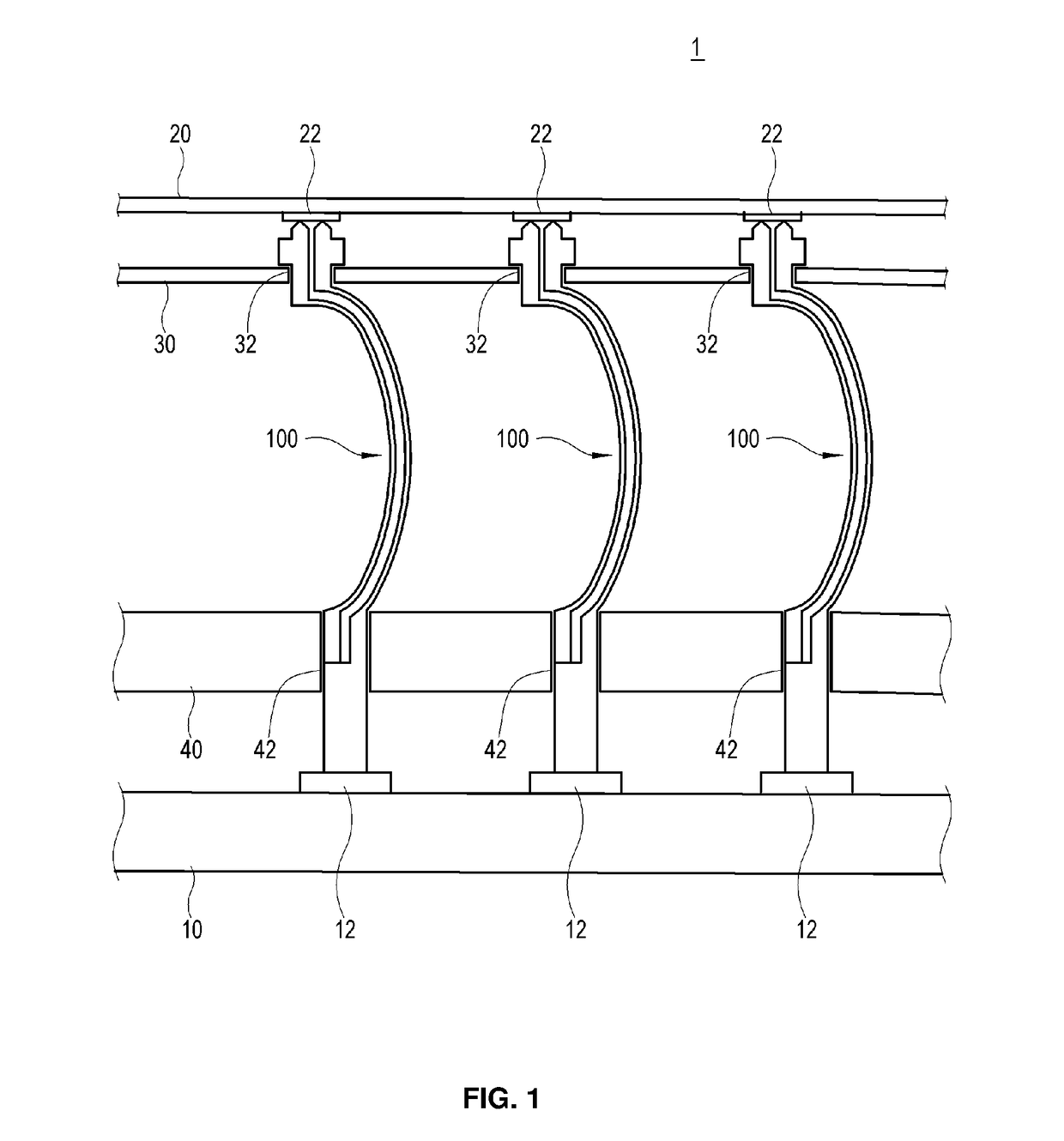
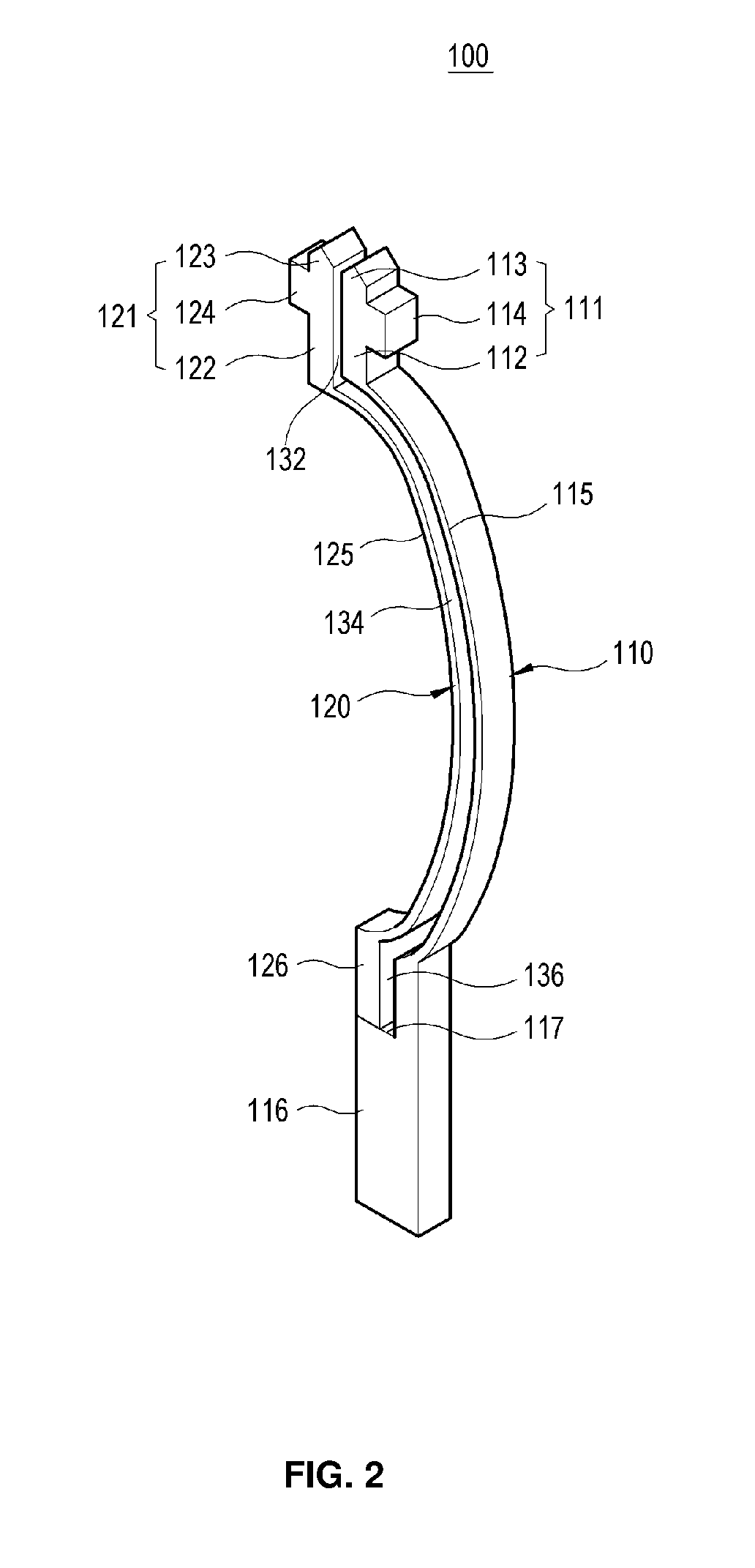
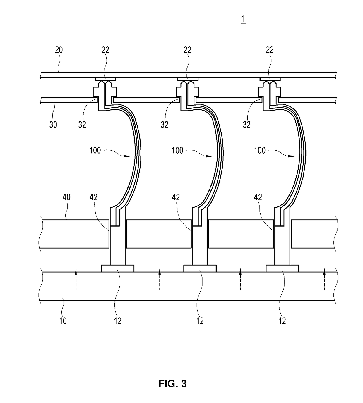
[0022]FIG. 1 is a cross-sectional view of a test device 1 using test probes according to the present disclosure, FIG. 2 is a perspective view of the test probe 100 of FIG. 1, and FIG. 3 is a cross-sectional view of showing that the test probe 100 of FIG. 1 is pressed against an object 10 to be tested during the test. As shown therein, the test device 1 includes a first support member 30 having a plurality of terminal holes 32, a second support member 40 arranged in parallel with the first support member 30 and having a plurality of plurality of guide holes 42, and a plurality of test probe 100.

[0023]The first support member 30 is provided as an insulating member shaped like a plate, and has the plurality of terminal holes 32 in which first ends of the main contact probe 110 and the sub contact probe 120 are respectively inserted.

[0024]The second support member 40 is arranged in parallel with the first support member 30 leaving a space therebetween. The second support member 40 is pr...

second embodiment

[0037]FIG. 4 is a perspective view of a test probe 200 according to the present disclosure. The test probe 200 is provided as a conductive member shaped like a plate having a predetermined thickness, and electrically connects two contact points, for example, the terminal 12 of the object 10 to be tested and the pad terminal 22 of the interposer 20. Of course, the test probe 200 may be applied for the purpose of electrically connecting any two contact points as well as the electric connection between the object 10 to be tested and the interposer 20.

[0038]The test probe 200 includes a main contact probe 210, the opposite ends of which are inserted in the terminal hole 32 and the guide hole 42, and a sub contact probe 220, the opposite ends of which are inserted together with the main contact probe 210 into the terminal hole 32 and the guide hole 42. The main contact probe 210 and the sub contact probe 220 are separated leaving a space based on slots 232, 234 and 236, or may be optiona...

third embodiment

[0049]FIG. 5 is a perspective view of a test probe 300 according to the present disclosure. As shown therein, the test probe 300 includes a main contact probe 310 and a sub contact probe 320. The main contact probe 310 includes a main terminal contact portion 311, a main elastic deformation portion 315, and a main sliding contact portion 316. The sub contact probe 320 includes a sub terminal contact portion 321, a sub elastic deformation portion 325 and a sub sliding contact portion 326. Below, the main contact probe 310 and the sub contact probe 320 have similar structures to those of the test probe 100 of FIG. 2, and thus repetitive descriptions thereof will be avoided. The main contact probe 310 and the sub contact probe 320 are separated from each other in a lengthwise direction by first to third slots 332, 334 and 336.

[0050]The main contact probe 310 and the sub contact probe 320 include two first and second engagement portions 340 and 350. The first engagement portion 340 incl...


PUM


Abstract

A test device for testing electric characteristics of an object to be tested. The test device includes: a first support member comprising a plurality of guide holes; a second support member comprising a plurality of terminal holes and arranged to be spaced apart from and in parallel with the first support member; a plurality of main contact probes; and a plurality of sub contact probes arranged to be adjacent to the main contact probes along a lengthwise direction. According to the present disclosure, contact reliability is improved by multi contact with the terminal of the test circuit board (interposer) and/or the object to be tested.

Description

REFERENCE TO RELATED APPLICATIONS[0001]This application claims the priority benefit of Korean Patent Application No. 10-2017-0099057 filed on Aug. 4, 2017, the entire contents of which are incorporated herein by reference.FIELD OF THE INVENTION[0002]The present disclosure relates to a test device for testing electric characteristics of a semiconductor or the like object to be tested.BACKGROUND OF THE INVENTION[0003]As a test device for testing electric characteristics of a semiconductor wafer or the like object to be tested, a probe card including a plurality of probes for electrical connection between a tested contact point of the object to be tested and a testing contact point of a test circuit has been used.[0004]With development of technology, the semiconductor wafer has become larger and a semiconductor has become smaller. As the number of semiconductor pads formable on one sheet of semiconductor wafer increases, a distance between semiconductor pads gets closer. Like this, a h...

Claims


Application Information

Patent Timeline
IPC IPC(8): G01R1/073G01R1/067
CPCG01R1/07371G01R1/06716G01R1/07342G01R1/06733G01R1/07357G01R31/2601G01R1/06738G01R1/0491G01R1/07307G01R31/2831
Inventor PARK, UNG-GI
Owner LEENO INDAL
Why Eureka
Try Eureka