Pixel circuit for top-emitting amoled panel and driving method thereof

a top-emitting amoled, pixel circuit technology, applied in the field of display techniques, can solve the problems of serious ir drop and greatly restricted aperture area of the bottom-emitting amoled, and achieve the effect of reducing ir voltage drop and increasing power consumption

Active Publication Date: 2019-02-28
SHENZHEN CHINA STAR OPTOELECTRONICS SEMICON DISPLAY TECH CO LTD
View PDF0 Cites 3 Cited by
  • Summary
  • Abstract
  • Description
  • Claims
  • Application Information

AI Technical Summary

Benefits of technology

[0040]In summary, the pixel circuit for top-emitting AMOLED panel and driving method of the present invention can effectively relieve the IR voltage drop caused by impedance increase of the transparent cathode and solve the circuit failure problem caused by VSS voltage raise as well as keeping the voltage difference between VDD and VSS without increasing power consumption. As such, the present invention is applicable to large-size top-emitting AMOLED panel.

Problems solved by technology

As the resolution increases, the aperture area of the bottom-emitting AMOLED is greatly restricted.
The transparent cathode of the current large-size top-emitting AMOLED panel has a high impedance, resulting in serious IR drop.

Method used


Image

  • Pixel circuit for top-emitting amoled panel and driving method thereof
  • Pixel circuit for top-emitting amoled panel and driving method thereof
  • Pixel circuit for top-emitting amoled panel and driving method thereof

Examples


Embodiment Construction

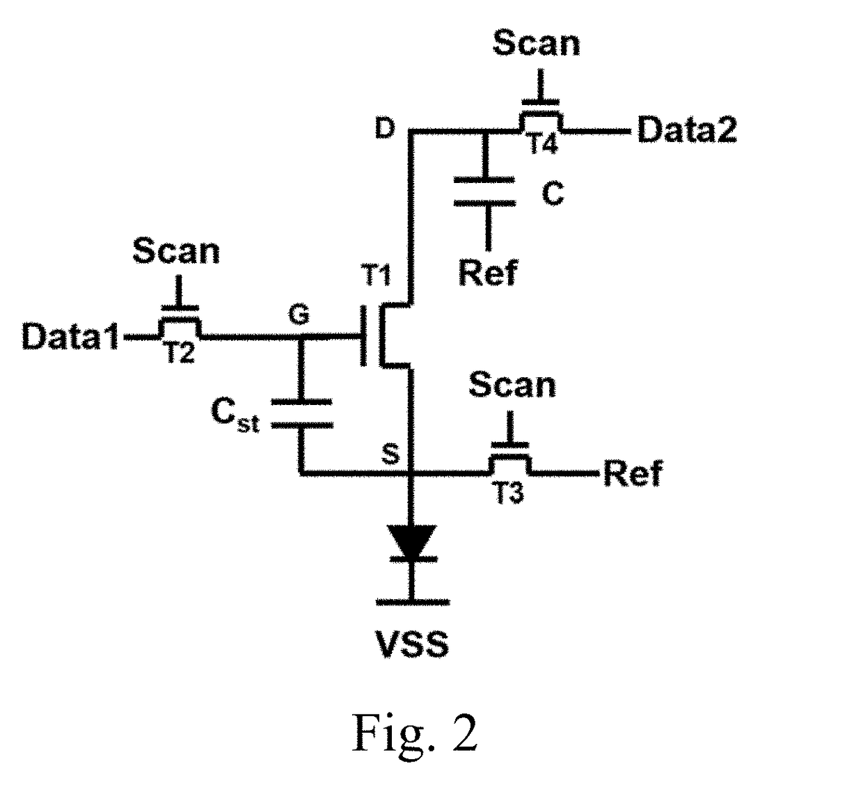
[0046]Referring to FIG. 2 and FIG. 3, FIG. 2 is a schematic view showing the structure of a preferred embodiment of the pixel circuit for top-emitting AMOLED panel of the present invention; FIG. 3 is a schematic view showing the signal timing sequence of a preferred embodiment of the pixel circuit for top-emitting AMOLED panel of the present invention. The preferred embodiment is a 4T2C pixel circuit, comprising: four TFTs T1-T4, and two capacitor Cst and C; wherein T1 serving as a driving TFT, T1, having a gate connected to node G, a source and a drain connected respectively to node S and node D; T2, having a gate connected to scan signal Scan, a source and a drain connected respectively to node G and data signal Data1; T3, having a gate connected to scan signal Scan, a source and a drain connected respectively to node S and reference voltage Ref; T4, having a gate connected to scan signal Scan, a source and a drain connected respectively to node D and high voltage power source Dat...


PUM


Abstract

The invention discloses a pixel circuit for top-emitting AMOLED panel and driving method thereof. The pixel circuit comprises: first TFT (T1), connected to first node(G), second node(S) and third node(D); second TFT(T2), connected to scan signal(Scan), first node(G) and data signal(Data1); third TFT(T3), connected to scan signal(Scan), second node(S) and reference voltage(Ref); fourth TFT(T4), connected to scan signal(Scan), third node(D) and high voltage power source(Data2); first capacitor(Cst), connected to first node(G) and second node(S); second capacitor(C), connected respectively to third node(D) and reference voltage(Ref); OLED, connected to second node(S) and low voltage power source(VSS); the voltage difference between high voltage power source(Data2) and low voltage power source(VSS) maintaining unchanged. The invention also provides a corresponding driving method. The invention can effectively relieve the IR voltage drop caused by increased impendence of the transparent cathode.

Description

BACKGROUND OF THE INVENTION1. Field of the Invention[0001]The present invention relates to the field of display techniques, and in particular to a pixel circuit for top-emitting AMOLED panel and driving method thereof.2. The Related Arts[0002]The organic light-emitting diode (OLED) has the advantages of low power consumption, wide color gamut, high brightness, high resolution, wide viewing angle, and fast response time, and attracts much attention.[0003]The driving types of OLED can be divided, according to the driving method, into the passive matrix OLED (PMOLED) and active matrix OLED (AMOLED); wherein the AMOLED provides the advantages of pixels arranged in an array, self-luminous, and high luminous efficiency and is commonly used for high definition large-size display. Based on the light-emission direction, the OLED can be either bottom-emitting type or top-emitting type. The light emitted from the top of the element for top-emitting OLED, and has a higher aperture ratio.[0004]T...

Claims


Application Information

Patent Timeline
Patent Type & Authority Applications(United States)
IPC IPC(8): G09G3/3258G09G3/3266H01L27/32
CPCG09G3/3258G09G3/3266H01L27/3262G09G2320/0204G09G2300/0819H01L27/1225H01L29/78672H01L29/7869H01L2251/5315G09G3/3233G09G2300/0842G09G2300/0866H10K2102/3026G09G2300/0852G09G2300/0861G09G2320/045G09G2320/043H10K59/1213
Inventor HAN, BAIXIANG
Owner SHENZHEN CHINA STAR OPTOELECTRONICS SEMICON DISPLAY TECH CO LTD
Why Eureka
Try Eureka