Electroluminescent display device and driving method thereof

a technology of electric light and display panel, which is applied in the direction of semiconductor devices, electrical devices, instruments, etc., can solve the problems of vertical luminance non-uniformity or crosstalk on the display panel, picture quality, etc., and achieve the effect of minimizing voltage drops

Active Publication Date: 2019-02-28
LG DISPLAY CO LTD
View PDF6 Cites 25 Cited by
  • Summary
  • Abstract
  • Description
  • Claims
  • Application Information

AI Technical Summary

Benefits of technology

[0009]The inventors of the present specification recognized the aforementioned problems and devised a display panel for minimizing voltage drops on voltage-supply lines and invented a display device using the same.
[0010]An aspect of the present disclosure is to provide a pixel circuit electroluminescence display that can solve / address picture quality issues such as vertical luminance non-uniformity or crosstalk on the display panel by compensating for time-varying characteristics, with voltage drops on voltage supply lines taken into consideration, and an electroluminescence display comprising the same.
[0011]Another aspect of the present disclosure is to provide an electroluminescence display that can achieve a high resolution by efficiently designing a gate driver providing gate signals applied to subpixels and a circuit providing a reference voltage.

Problems solved by technology

However, some of the commonly proposed compensation methods do not take drops in the voltage applied to the subpixels into consideration, which result in picture quality issues such as vertical luminance non-uniformity or crosstalk on the display panel.

Method used


Image

  • Electroluminescent display device and driving method thereof
  • Electroluminescent display device and driving method thereof
  • Electroluminescent display device and driving method thereof

Examples


first embodiment

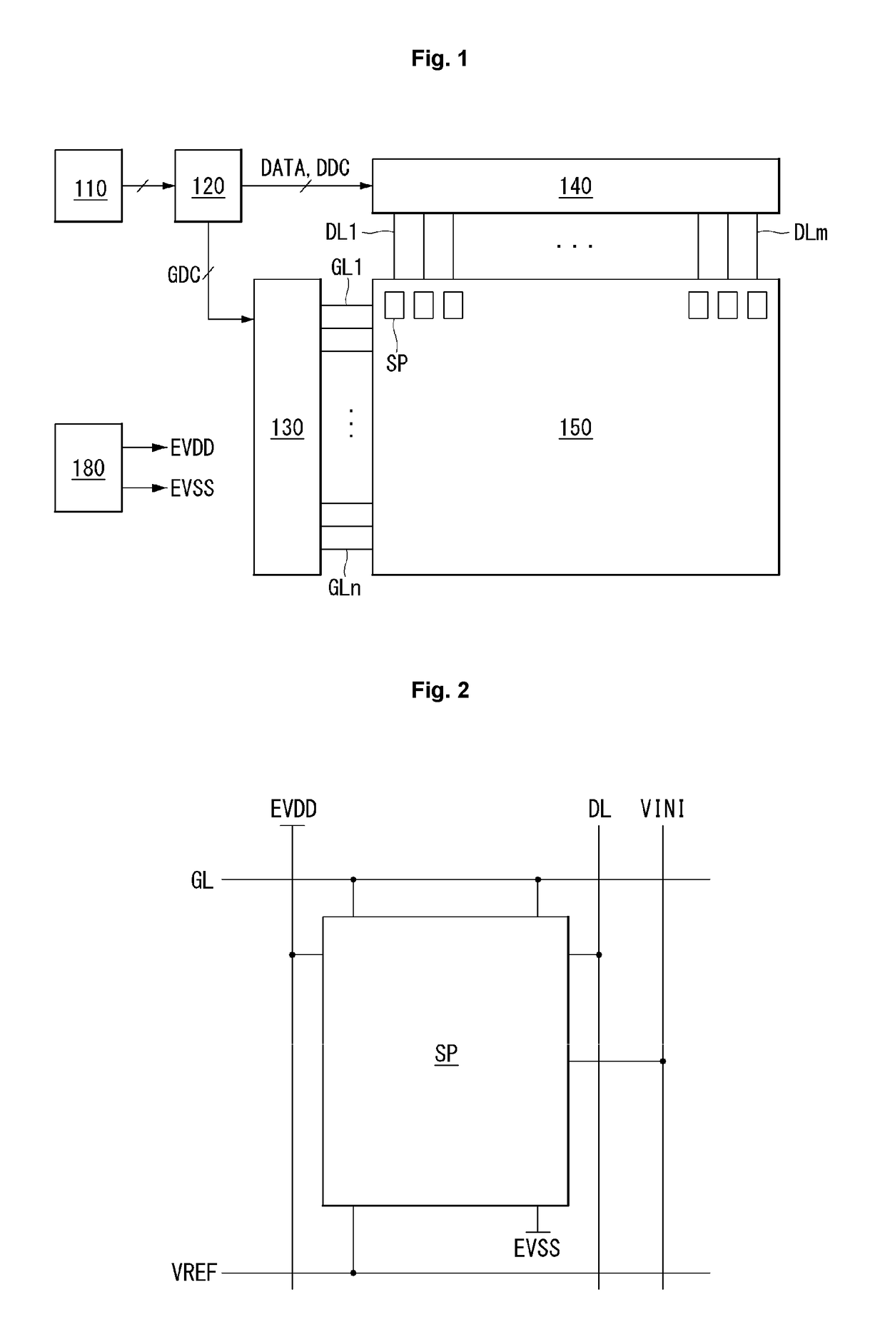
[0081]FIG. 6 is a block diagram of a display panel which schematically illustrates an electroluminescence display according to an embodiment of the present disclosure. FIG. 7 is a waveform diagram explaining some of the drive characteristics of the subpixel of FIG. 6.

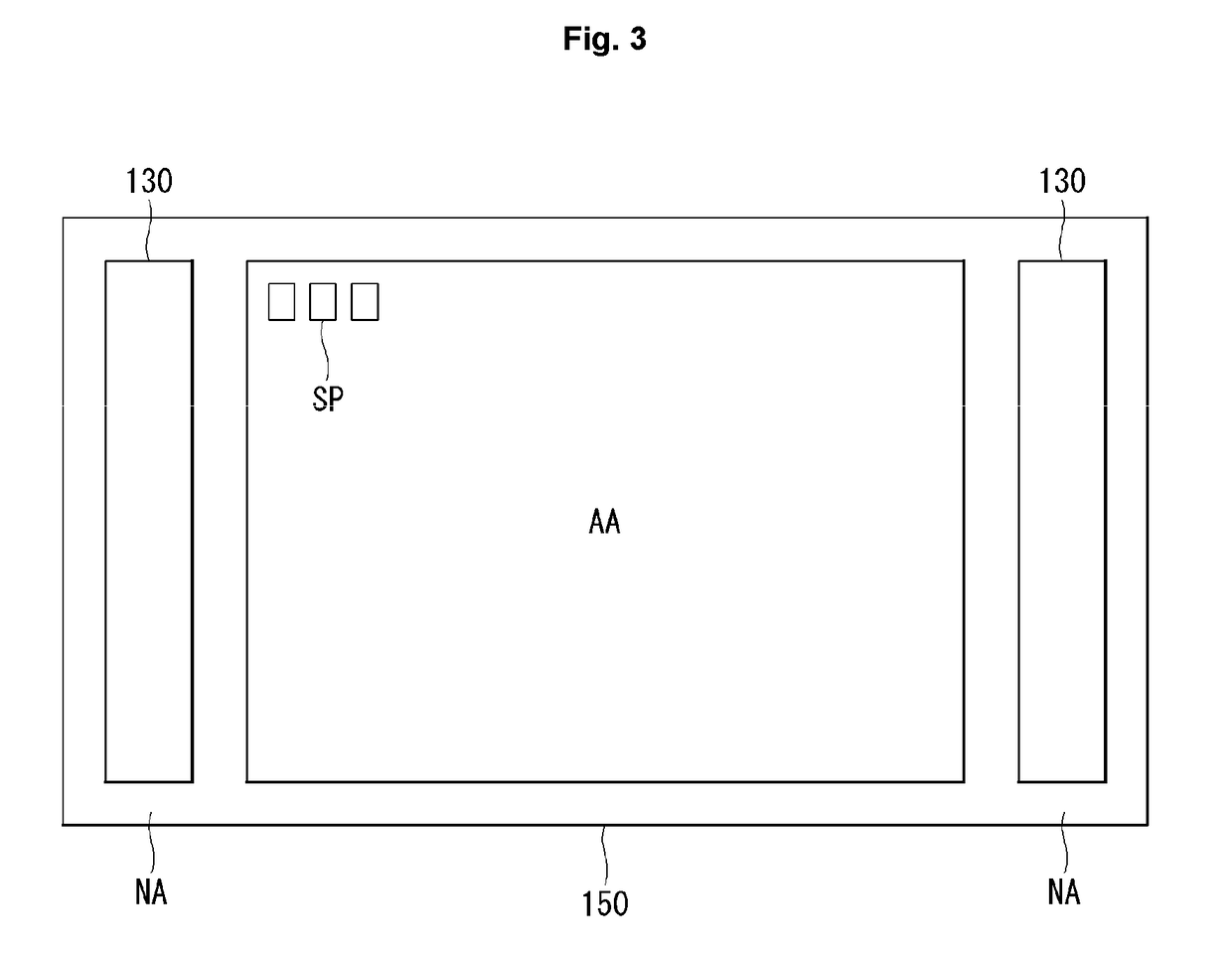
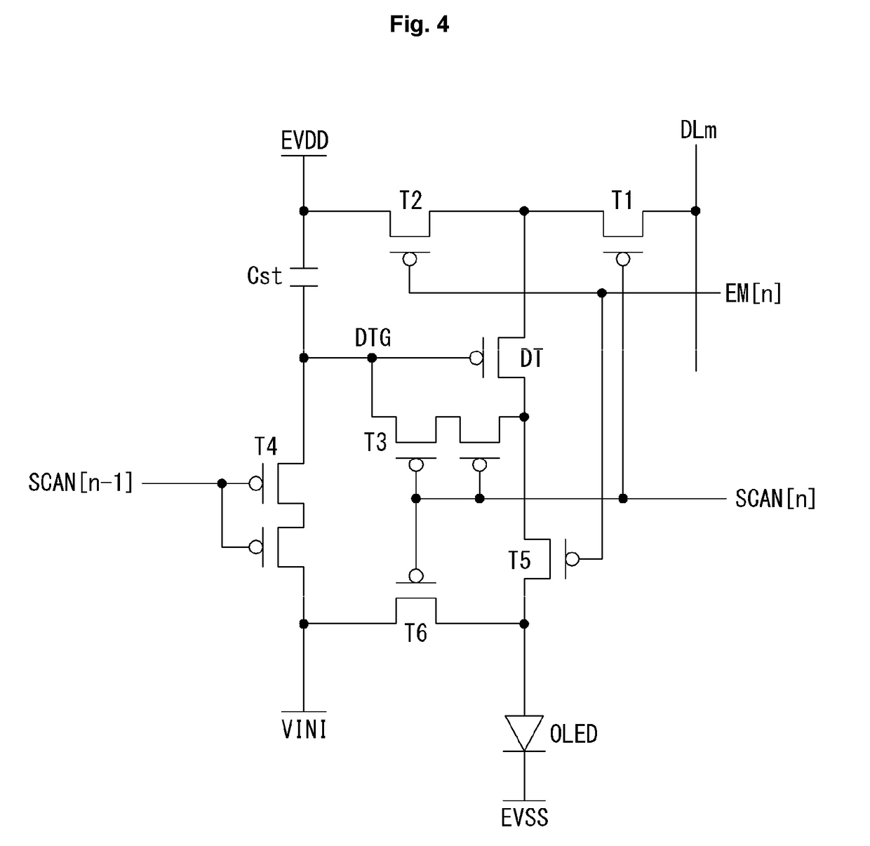
[0082]As illustrated in FIGS. 6 and 7, the electroluminescence display according to the first embodiment comprise an nth voltage transfer part VRD that performs an operation for transferring an externally applied voltage to subpixels so as to compensate for voltage drop in the first power supply voltage applied to the nth subpixels SPs. Here, the term “externally” refers to the outside of the display area AA. The term voltage transfer part VRD is used interchangeable with the term voltage transfer transistor hereinafter, unless otherwise stated. The voltage transfer part VRD may represent at least one voltage transfer transistor that is located in the non-display area NA, wherein a gate of the at least one voltage trans...

second embodiment

[0125]FIG. 17 is a diagram of the configuration of a display panel which schematically explains an electroluminescence display according to a second embodiment of the present disclosure. FIG. 18 is a waveform diagram explaining some of the drive characteristics of the subpixel circuit of FIG. 17. The second embodiment of the present disclosure is a modification of the first embodiment, so redundancies between the first and second embodiments will be omitted or described briefly.

[0126]As illustrated in FIGS. 17 and 18, the electroluminescence display according to the second embodiment comprise an Nth voltage transfer part VRD that performs an operation for transferring an externally applied voltage to subpixels so as to compensate for voltage drop in the first power supply voltage applied to the nth subpixels SPs. Here, the term “externally” refers to the outside of the display area AA.

[0127]The nth voltage transfer part VRD is placed in the non-display area NA. The nth voltage trans...

third embodiment

[0147]FIG. 19 is a diagram of the configuration of a display panel which schematically explains an electroluminescence display according to a third embodiment of the present disclosure. FIG. 20 is a waveform diagram explaining some of the drive characteristics of the subpixel circuit of FIG. 19. The third embodiment of the present disclosure is a modification of the first and / or second embodiments, so redundancies between the third embodiment and the first and second embodiments will be omitted or described briefly.

[0148]As illustrated in FIGS. 19 and 20, the electroluminescence display according to the third embodiment comprise an nth voltage transfer part VRD that performs an operation for transferring an externally applied voltage to subpixels so as to compensate for voltage drop in the first power supply voltage applied to the nth subpixels SPs. Here, the term “externally” refers to the outside of the display area AA.

[0149]The nth voltage transfer part VRD is placed in the non-d...


PUM


Abstract

There is provided an electroluminescence display device comprising a display panel having a display area where images are displayed and a non-display area where images are not displayed, a subpixel located in the display area, and a voltage transfer part that is located in the non-display area and transfers a reference voltage to the subpixel in response to a signal applied from outside the display panel or a signal generated on the display panel.

Description

[0001]This application claims the priority benefit of Korean Patent Application No. 10-2017-0111225, filed on Aug. 31, 2017, and No. 10-2017-0135720, filed on Oct. 19, 2017, the entire contents of all these applications are incorporated herein by reference for all purposes as if fully set forth herein.BACKGROUNDField[0002]The present disclosure relates to an electroluminescence display and a driving method thereof.Related Art[0003]The market for displays which act as an intermediary between users and information is growing with the development of information technology. Thus, different types of display devices such as electroluminescence displays, liquid crystal displays, and quantum dot displays are increasingly used.[0004]A display device comprises a display panel comprising a plurality of subpixels and a driving unit that drives the display panel. The driving unit comprises a gate driver that supplies gate signals to the display panel and a data driver that supplies data signals ...

Claims


Application Information

Patent Timeline
Patent Type & Authority Applications(United States)
IPC IPC(8): G09G3/3266H01L51/52G09G3/3291G09G3/3258H01L27/32
CPCG09G3/3266H01L51/5206H01L51/5221G09G3/3291G09G3/3258H01L27/3265H01L27/3276G09G3/3233G09G2300/0819G09G2300/0842G09G2300/0861G09G2300/0876G09G2310/0251G09G2310/06G09G2320/0233G09G2320/045G09G2330/025H10K50/81H10K50/82H10K59/131H10K59/1216
Inventor KIM, JAESUNGYOO, JUHNSUKKIM, JUNGCHULKONG, CHUNGSIKSHIN, MIHEEHAN, HONGGYU
Owner LG DISPLAY CO LTD
Why Eureka
Try Eureka