

Display device
- Summary
- Abstract
- Description
- Claims
- Application Information
AI Technical Summary
Benefits of technology
Problems solved by technology
Method used
Image

Examples
embodiments
[0096]More specific embodiments of the present invention will now be described with reference to the drawings. While the embodiments below illustrate implementations where the display device of the present invention is a liquid crystal display device, the present invention is not limited to liquid crystal display devices and may be used in any display device using an active matrix substrate. Typically, the display device of the present invention may be a touch panel-equipped display device having photosensors to detect an object located close to the screen for an input operation, or a two-way communication display device including display and image capturing capabilities.
[0097]For ease of explanation, the drawings referred to below schematically show only those of the components of the embodiments of the present invention that are necessary to illustrate the present invention. Accordingly, the display device of the present invention may include an optional component not shown in the...
first embodiment
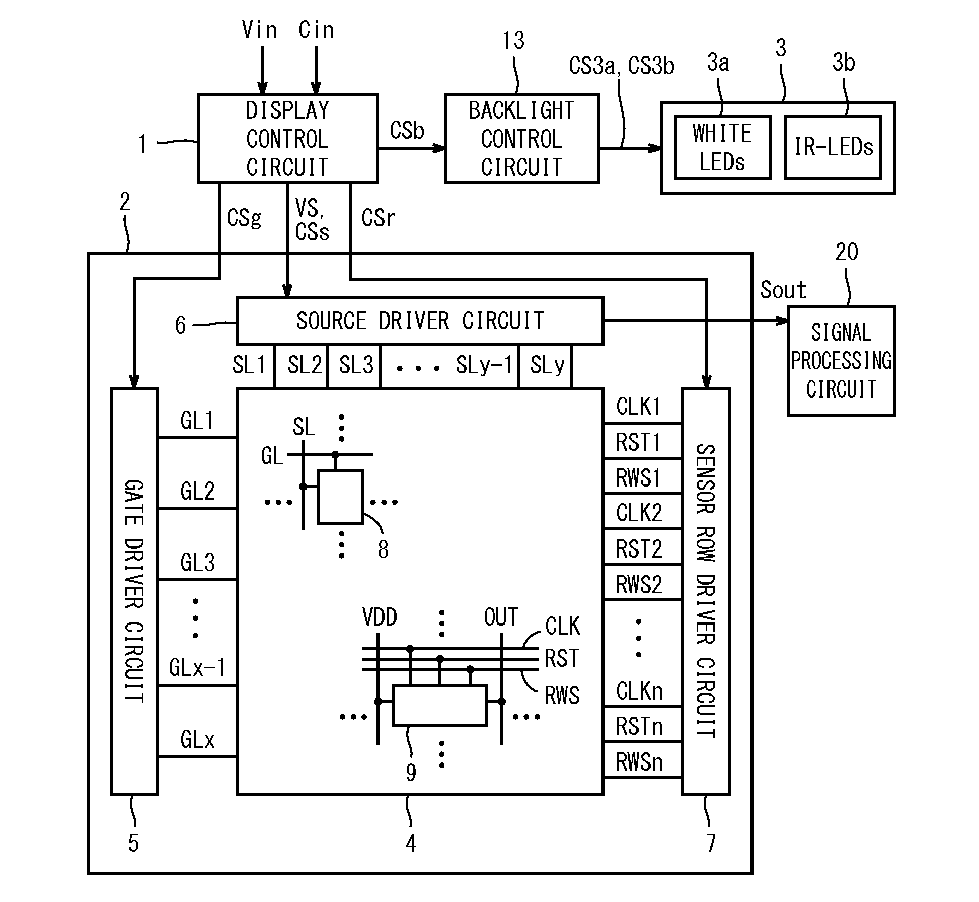
[0098]FIG. 1 is a block diagram of a display device according to an embodiment of the present invention. The display device shown in FIG. 1 includes a display control circuit 1, display panel 2, backlight 3 and backlight control circuit 13 (light source control circuit). The display panel 2 includes a pixel region 4, gate driver circuit 5, source driver circuit 6 (amplifier circuit) and sensor row driver circuit 7 (sensor drive circuit). The pixel region 4 includes a plurality of display pixel circuits 8 and a plurality of sensor pixel circuits 9 (photosensors). The display device has the capability of displaying an image on the display panel 2 and the capability of sensing light entering the display panel 2. In the following description, x is an integer not smaller than 2, y is a multiple of 3, m and n are even numbers, and the frame rate of the display device is 60 frames per second.
[0099]The display device shown in FIG. 1 is supplied with a video signal Vin and a timing control s...
second embodiment
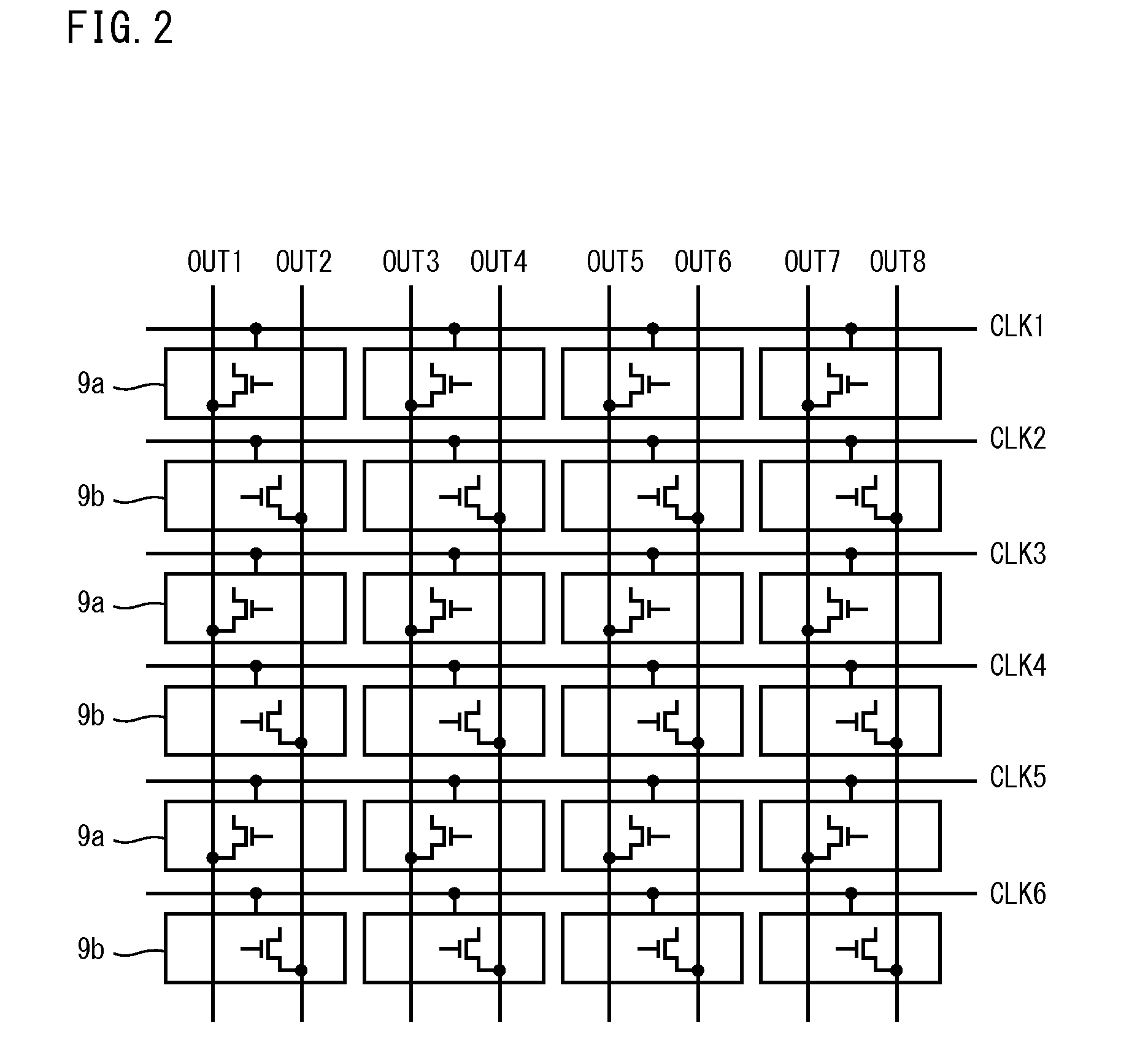
[0161]FIG. 24 is a circuit diagram of a pixel circuit according to a second embodiment of the present invention. The pixel circuit 30 shown in FIG. 24 includes transistors T1a, T1b, M1a and M1b, a photodiode D1, and capacitors C1a and C1b. The transistors T1a, T1b, M1a and M1b are n-type TFTs. In FIG. 24, the left half corresponds to the first pixel circuit while the right half corresponds to the second pixel circuit. The pixel circuit 30 is connected with clock lines CLKa and CLKb, a reset line RST, readout lines RWS, power supply lines VDDa and VDDb and output lines OUTa and OUTb.
[0162]As shown in FIG. 24, the photodiode D1 has an anode connected with the reset line RST and a cathode connected with the sources of the transistors T1a and T1b. The transistor T1a has a gate connected with the clock line CLKa and a drain connected with the gate of the transistor M1a. The transistor M1a has a drain connected with the power supply line VDDa and a source connected with the output line OU...
PUM
 Abstract
Description
Claims
Application Information