Most compact flotox-based combo NVM design without sacrificing EEPROM endurance cycles for 1-die data and code storage

a combo nvm and endurance cycle technology, applied in static storage, digital storage, instruments, etc., can solve the problems of extremely high data changing rate, no flash-based combo nvm chip can meet the criteria now and for the future, etc., to achieve more reliable programming, and high data storage application changing rate

Inactive Publication Date: 2012-03-15
APLUS FLASH TECH
View PDF3 Cites 42 Cited by
  • Summary
  • Abstract
  • Description
  • Claims
  • Application Information

AI Technical Summary

Benefits of technology

[0109]The first (1st) object of this invention discloses a novel 2T FLOTOX-based EEPROM cell array structure, which is preferably formed by removing a HV ST transistor and GBL physically from each byte but keep a common source node for eight cells of the traditional EEPROM cell array for byte size reduction. The byte layout area reduction does not sacrifice the P / E endurance performance performed in unit of byte and page for those high changing rate of data storage application.
[0110]The second (2nd) object of this invention similarly discloses a novel 2T FLOTOX-based EEPROM cell array structure, which is preferably formed by removing a HV ST transistor and GBL and common SL physically from each byte to eliminate the voltage drop happening to the common CG of the select byte. The traditional common SL is preferably replaced by eight pairs of BLs and SLs for more reliable programming of the traditional EEPROM cell array plus no GBL is for byte size reduction. Like 1st objective, the byte layout area reduction does not sacrifice the P / E endurance performance performed in unit of byte and page for those high changing rate of data storage application.
[0111]The third (3rd) object of this invention discloses a novel set of positive erase and erase inhibit bias voltage combinations for WLs, CGs, BLs and SLs for the selected and unselected bytes in the selected page (or WL) and unselected pages (or WLs) of the preferable 2T FLOTOX-based EEPROM cell array structures without GBL of the present invention. The preferable erase and erase voltages are coupled directly from BLs to the selected cells' channel regions along with the floating of selected SLs to effectively reduce the voltage drop between gate and channel of EEPROM cells so that FN-tunneling effect would not happen or drastically reduced. Like the traditional EEPROM, the desired erase Vt is set to be positive about +2.0V.
[0112]The fourth (4th) object of this invention discloses a novel set of positive program and program inhibit bias voltage combinations for WLs, CGs, BLs and SLs for the selected and unselected bytes in the selected page (WL) and unselected pages (WLs) of the preferable 2T FLOTOX-based EEPROM cell array structures without GBL of the present invention. The preferable erase and erase voltages are coupled directly from BLs to the selected cells' channel regions along with the floating of selected SLs to effectively reduce the voltage drop between gate and channel of EEPROM cells so that FN-tunneling effect would not happen or drastically reduced. Like the traditional EEPROM, The desired erase Vt is set to be −2.0V that is negative below 0V.
[0113]The fifth (5th) object of this invention discloses a novel set of positive erase and erase inhibit bias voltage combinations for WLs, CGs, BLs and SLs for the selected and unselected bytes in the selected page (or WL) and unselected pages (or WLs) of the preferable 2T FLOTOX-based EEPROM cell array structures without GBL of the present invention. But unlike the 3rd objective, the preferable erase and erase inhibit voltages are coupled directly from SLs to the selected cells' channel regions along with the floating of selected SLs to effectively reduce the voltage drop between gate and channel of EEPROM cells so that FN-tunneling effect would not happen or drastically reduced. Like the traditional EEPROM, The desired erase Vt is set to be positive about +2.0V.
[0114]The sixth (6th) object of this invention discloses a novel set of positive program and program inhibit bias voltage combinations for WLs, CGs, BLs and SLs for the selected and unselected bytes in the selected page (WL) and unselected pages (WLs) of the preferable 2T FLOTOX-based EEPROM cell array structures without GBL of the present invention. But unlike the 4th objective, the preferable erase and erase voltages are coupled directly from SLs to the selected cells' channel regions along with the floating of selected SLs to effectively reduce the voltage drop between gate and channel of EEPROM cells so that FN-tunneling effect would not happen or drastically reduced. Like the traditional EEPROM, The desired erase Vt is set to be −2.0V which is negative below 0V.

Problems solved by technology

As a result, when EEPROM's strict spec requiring 1M P / E cycles in unit of byte for 10-year product cycle, none of those Flash-based combo NVM chip can meet the criteria now and for-seeable future.
The Data-oriented combo chip design means NAND and NOR have to use the existing Flotox-based EEPROM cell and process to design on the same chip without degrading any EEPROM quality and performance, due to an extremely high data changing rate in many practical applications.

Method used


Image

  • Most compact flotox-based combo NVM design without sacrificing EEPROM endurance cycles for 1-die data and code storage
  • Most compact flotox-based combo NVM design without sacrificing EEPROM endurance cycles for 1-die data and code storage
  • Most compact flotox-based combo NVM design without sacrificing EEPROM endurance cycles for 1-die data and code storage

Examples


Embodiment Construction

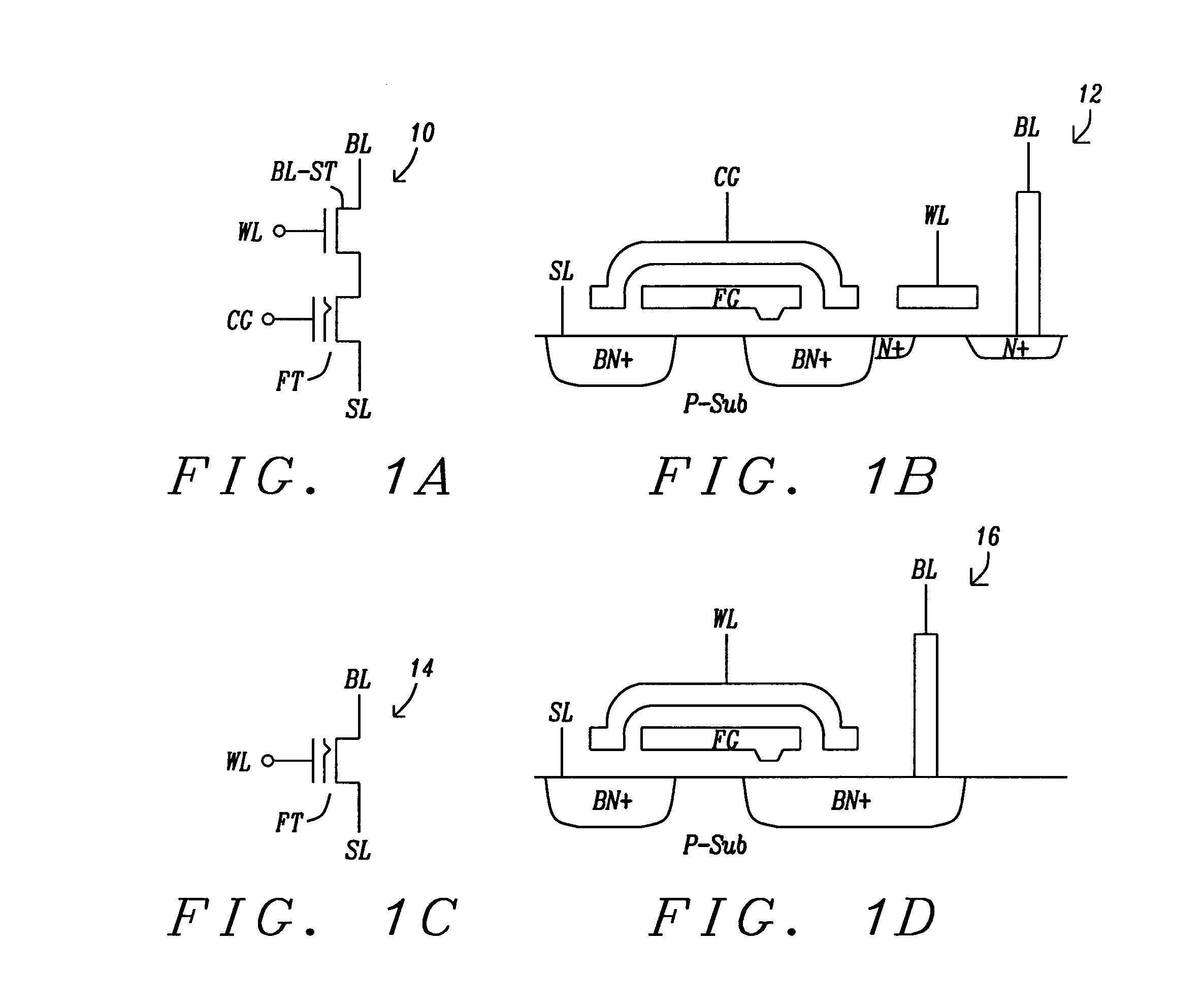
[0124]FIG. 1A, 10, shows a typical Flotox-based 2T EEPROM cell circuit of both prior art and the present invention. It comprises of two HV NMOS transistors such as 1-poly BL-ST transistor and 2-poly floating-gate FT transistor. The top BL-ST transistor is called the Bitline-Select transistor and is used to protect the bottom FT storage cell from being disturbed when 16V is applied to BL during the program operation. The source of FT is denoted as SL, and the drain of the BL-ST is denoted as BL. The gate of BL-ST is denoted as WL, while the gate of FT is denoted as CG. Note, WL stands for word line and CG stands for Control-gate of the floating-transistor. This 2T EEPROM cell typical has cell size of 100λ2 and is the largest NVM cell size so far. The on-chip operation needs maximum positive 16V VPP1 as shown in the attached tables.

[0125]FIG. 1B, 12, shows the cross-sectional view of the 2T EEPRPM cell shown in FIG. 1A. The CG on top is formed by the Poly2 layer used in peripheral dev...


PUM


Abstract

Disclosed is a low-cost hybrid storage solution that allows Code like sector-alterable NOR and Data like block-alterable NAND and byte-alterable EEPROM being integrated on a same die. The disclosed combo NVM design of the present invention is a truly Data-oriented NVM design that allows 2T-EEPROM to integrate both 0.5T-NAND and 1T-NOR without sacrificing any EEPROM's byte-write performance in the same die. The invention provides several new embodiment sets of preferable bias conditions of Program, Program-Inhibit, Erase and Erase-Inhibit for operating bit-write, byte-write, sector-write and page-write for several preferable Flotox-based EEPROM, NOR and NAND or combo NVM arrays that include types of shared SL, 8-pair BLs and SLS, with or without GBL, normally Erased Vt and Programmed Vt, or the reversed Erased-Vt or Programmed-Vt, etc. Further disclosed is a flexible X-decoder design to allow the flexible selection of pages to be erased to save erase time. Also disclosed is using on-chip negative voltage for FT's gate along with the less positive HV applied to FTs' channel region for same write performance but with the benefits of channel length reduction in cell and less BVDS electric requirement in peripheral devices for more scalable manufacturing process.

Description

[0001]This application claims priority to U.S. Provisional Patent Application Ser. No. 61 / 403,187, filed Sep. 9, 2010, which is owned by a common assignee, and which is herein incorporated by reference in its entirety.CROSS-REFERENCE TO RELATED APPLICATIONS[0002]This application is related to the following US patent applications:[0003]AP08-004, titled “NAND Based NMOS NOR Flash Memory Cell, a NAND Based NMOS NOR Flash Memory Array, and a Method of forming a NAND Based NMOS NOR Flash Memory Array”, utility Ser. No. 12 / 387,771, utility filing date May 7, 2009,[0004]AP08-001, titled “An Integrated SRAM and FLOTOX EEPROM Memory Device”, utility Ser. No. 12 / 319,241, utility filing date Jan. 5, 2009,[0005]AP09-004, titled “A Novel High Speed Two Transistor / Two Bit NOR Read Only Memory”, utility Ser. No. 12 / 804,156, utility filing date Jul. 15, 2010, and[0006]AP09-011, titled “A Novel Cell Array for Highly-Scalable, Byte-Alterable, Two-Transistor FLOTOX EEPROM Non-Volatile Memory”, utility...

Claims


Application Information

Patent Timeline
Patent Type & Authority Applications(United States)
IPC IPC(8): G11C16/10G11C16/04
CPCG11C16/0433G11C16/3436G11C16/12G11C11/005
Inventor LEE, PETER WUNGHSU, FU-CHANG
Owner APLUS FLASH TECH
Why Eureka
Try Eureka