Semiconductor integrated circuit device and its power supply wiring method

a technology of integrated circuit devices and power supply wires, which is applied in the direction of semiconductor devices, semiconductor/solid-state device details, instruments, etc., can solve the problems of inability to achieve the conventional power supply wiring described above, inability to achieve sufficient mitigation of ir drop, and the current density of power supply wires may local exceed the tolerable current density, etc., to achieve the effect of improving stability

Inactive Publication Date: 2006-10-26
SANYO ELECTRIC CO LTD
View PDF0 Cites 47 Cited by
  • Summary
  • Abstract
  • Description
  • Claims
  • Application Information

AI Technical Summary

Benefits of technology

[0007] It is an object of the present invention to provide a semiconductor integrated circuit having improved stability and a method for wiring the power supply wiring of the same.
[0008] To achieve the above object, one aspect of the present invention is a semiconductor integrated circuit device including a circuit portion, a first power supply wire for supplying power to the circuit portion, and second power supply wires electrically connected to the first power supply wire. The semiconductor integrated circuit device includes at least one of width of each second power supply wire and an interval between the second power supply wires is set so as to mitigate voltage drop in the second power supply wires.
[0023] The present invention further provides a method for wiring a power supply of a semiconductor integrated circuit device including a circuit portion and a first power supply wire for supplying power to the circuit portion. The method includes the steps of providing second power supply wires electrically connected to the first power supply wire, and setting at least one of width of the second power supply wires and an interval of the second power supply wires to mitigate voltage drop in the second power supply wires.
[0032] In one embodiment, the main power piece is one of a plurality of main power pieces. The method includes when one main power piece partially overlaps at least one other main power piece, deleting a part including the overlapping region from the main power piece that has a long distance from the associated power supply portion to the overlapping region, moving the deleted part to a position that does not overlap another main power piece, and resetting the main power pieces to eliminate the overlapping region.

Problems solved by technology

An IR drop in the power supply wiring leads to low response speed and deficient operation of the logic gate and thus cannot be overlooked.
However, sufficient mitigation of the IR drop cannot be attained with the conventional power supply wiring described above due to the extended length of the wires and miniaturization of wires resulting from the rapid enlargement and integration of LSIs in recent years.
Furthermore, in parts of a logic circuit portion having relatively large power consumption, the current density of the power supply wires may locally exceed the tolerable current density.
Since excessive current density causes the generation of electromigration, restriction violations in the current density reduce the reliability of the LSI.

Method used


Image

  • Semiconductor integrated circuit device and its power supply wiring method
  • Semiconductor integrated circuit device and its power supply wiring method
  • Semiconductor integrated circuit device and its power supply wiring method

Examples


first modification

(First Modification)

[0142] Although the reinforcing power supply wire (power supply mesh) is arranged in accordance with the magnitude of the provisional IR drop value in the second embodiment, a wiring arrangement shown in FIG. 14 may be alternatively used in the reinforcing power supply wire. That is, in this modification the vertical reinforcing power supply wires 32 are basically arranged to substantially equalize the amount of power consumption in adjacent regions defined by the vertical reinforcing power supply wires 32. Similarly, the lateral reinforcing power supply wires 33 are basically arranged to substantially equalize the amount of power consumption in adjacent regions defined by the lateral reinforcing power supply wires 33.

[0143] The power supply wiring method of this modification is described below. FIG. 15 is a flowchart showing some of the procedures executed by an information processor to lay out the power supply wiring in the present modification. As shown in FI...

second modification

(Second Modification)

[0149] Any method for correcting the wiring positions of the vertical reinforcing power supply wires and lateral reinforcing power supply wires may be performed. For example, the processes of steps S213a1 through S213a8 shown in FIG. 18 may be substituted for the repeated processes (steps S207 to S213) in the second embodiment.

[0150] That is, when an IR drop exceeding the upper limit is generated in the first step S213 (S213: NO), the process of step S213a1 is performed rather than returning to step S207. In step S213a1, the vertical reinforcing power supply wires nearest the provisional IR drop peak position P on the IR drop map, that is, two (one set of) vertical reinforcing power supply wires 232 sandwiching the peak position therebetween, are selected. When there are a plurality of provisional IR drop peak positions, for example, the process selects the peak position that has the largest provisional IR drop value.

[0151] Specifically, as shown in FIG. 19, w...

third modification

(Third Modification)

[0160] The processes of steps S213b1 through S213b11 shown in FIG. 23 may be substituted for the repeated processes (steps S207 to S213) of the second embodiment as the process for correcting the wiring position of the vertical reinforcing power supply wires and lateral reinforcing power supply wires.

[0161] More specifically, when an IR drop exceeding the upper limit is generated in the first step S213 (S213: NO), the process of step S213b1 is performed rather than returning to step S207.

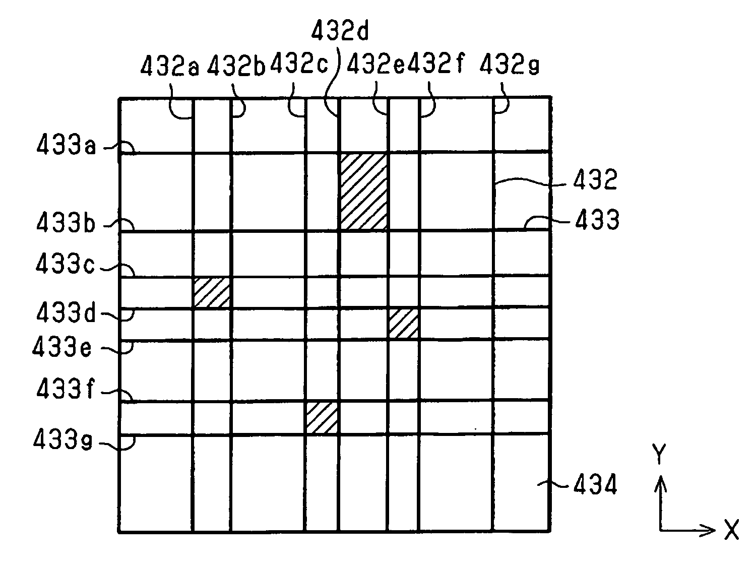
[0162] In the process of step S213b1, a lower limit value and upper limit value for the IR drop value (tolerable range) are set. In step S213b2, region C which has the lowest provisional IR drop value is selected from among the grid regions defined by the vertical reinforcing power supply wires 332 and lateral reinforcing power supply wires 333 (reinforcing power supply wires 331), as shown in FIG. 24. The provisional IR drop value of the grid region is the total of the provisi...


PUM


Abstract

The present invention discloses a power supply wiring method for stabilizing operation of a semiconductor integrated circuit device. A power supply mesh 24, which is arranged on an upper layer of a basic power supply wires 18 for supplying power to a logic circuit portion 13, includes vertical reinforcing power supply wires 22 and lateral reinforcing power supply wires 23. The widths of the vertical reinforcing power supply wires and lateral reinforcing power supply wires are optimized to mitigate IR drop or excessive current density in each division unit u0.

Description

FIELD OF THE INVENTION [0001] The present invention relates to a semiconductor integrated circuit device and method for wiring a power supply. BACKGROUND ART [0002] Advances in producing large-scale, highly integrated semiconductor integrated circuits (LSI) have resulted in outstanding voltage drops (IR drop) in logic circuits (for example, near the central area) caused by an increase in the resistance of power supply wiring, which is used to supply operation current to the logic circuit area. An IR drop in the power supply wiring leads to low response speed and deficient operation of the logic gate and thus cannot be overlooked. In a conventional LSI, to mitigate the IR drop, the total wiring width is increased by using reinforcing power supply wires in addition to basic power supply wire, which directly supply power to logic circuits. (See Japanese Laid-Open Patent Publication No. 2002-261245) [0003]FIG. 91 is a plan view showing power supply wiring for a conventional LSI. The LSI...

Claims


Application Information

Patent Timeline
Patent Type & Authority Applications(United States)
IPC IPC(8): G11C5/14H01L23/528
CPCH01L23/5286H01L2924/13091H01L24/06H01L2924/00H01L2924/14
Inventor SAITA, ATSUSHIMUKUNO, MAMORU
Owner SANYO ELECTRIC CO LTD
Why Eureka
Try Eureka