Method of forming vertical field effect transistors with self-aligned gates and gate extensions and the resulting structure

Active Publication Date: 2019-03-21
GLOBALFOUNDRIES US INC
View PDF0 Cites 7 Cited by
  • Summary
  • Abstract
  • Description
  • Claims
  • Application Information

AI Technical Summary

Benefits of technology

[0003]In view of the foregoing, disclosed herein are embodiments of a method of forming an integrated circuit (IC) that incorporates multiple vertical field effect transistors (VFETs) (e.g., in a VFET array). In the method, self-aligned gates for each pair of VFETs and a self-aligned gate extension for contacting those self-aligned gates are essentially simultaneously formed. The resulting gates wrap around a pair of semiconductor fins, which are in end-to-end alignment, and the resulting gate extension fills the space between adjacent ends

Problems solved by technology

Unfortunately, as the device density (i.e., the number of devices per unit area) included in IC design specifications continues to be increased, f

Method used


Image

  • Method of forming vertical field effect transistors with self-aligned gates and gate extensions and the resulting structure
  • Method of forming vertical field effect transistors with self-aligned gates and gate extensions and the resulting structure
  • Method of forming vertical field effect transistors with self-aligned gates and gate extensions and the resulting structure

Examples


Embodiment Construction

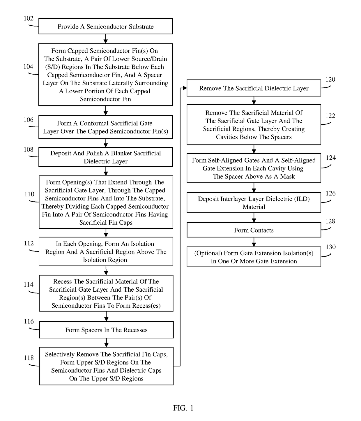
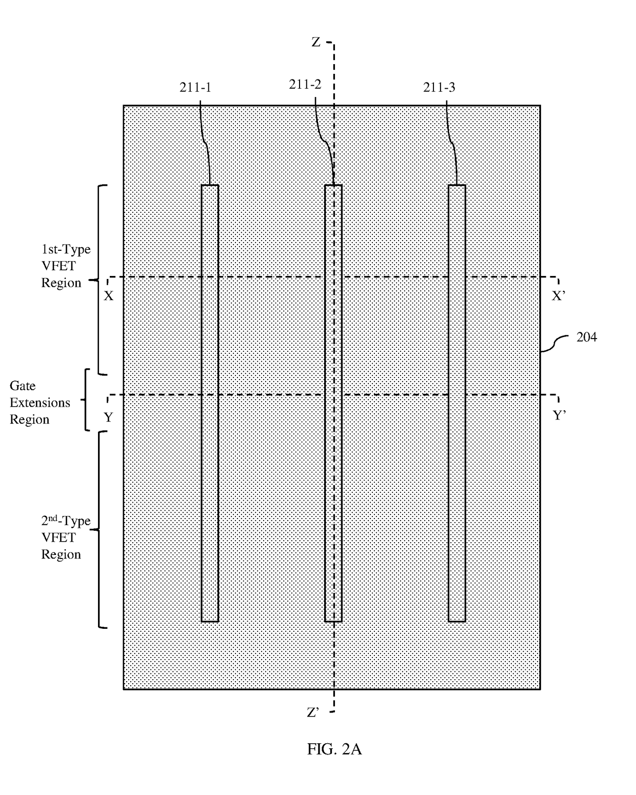
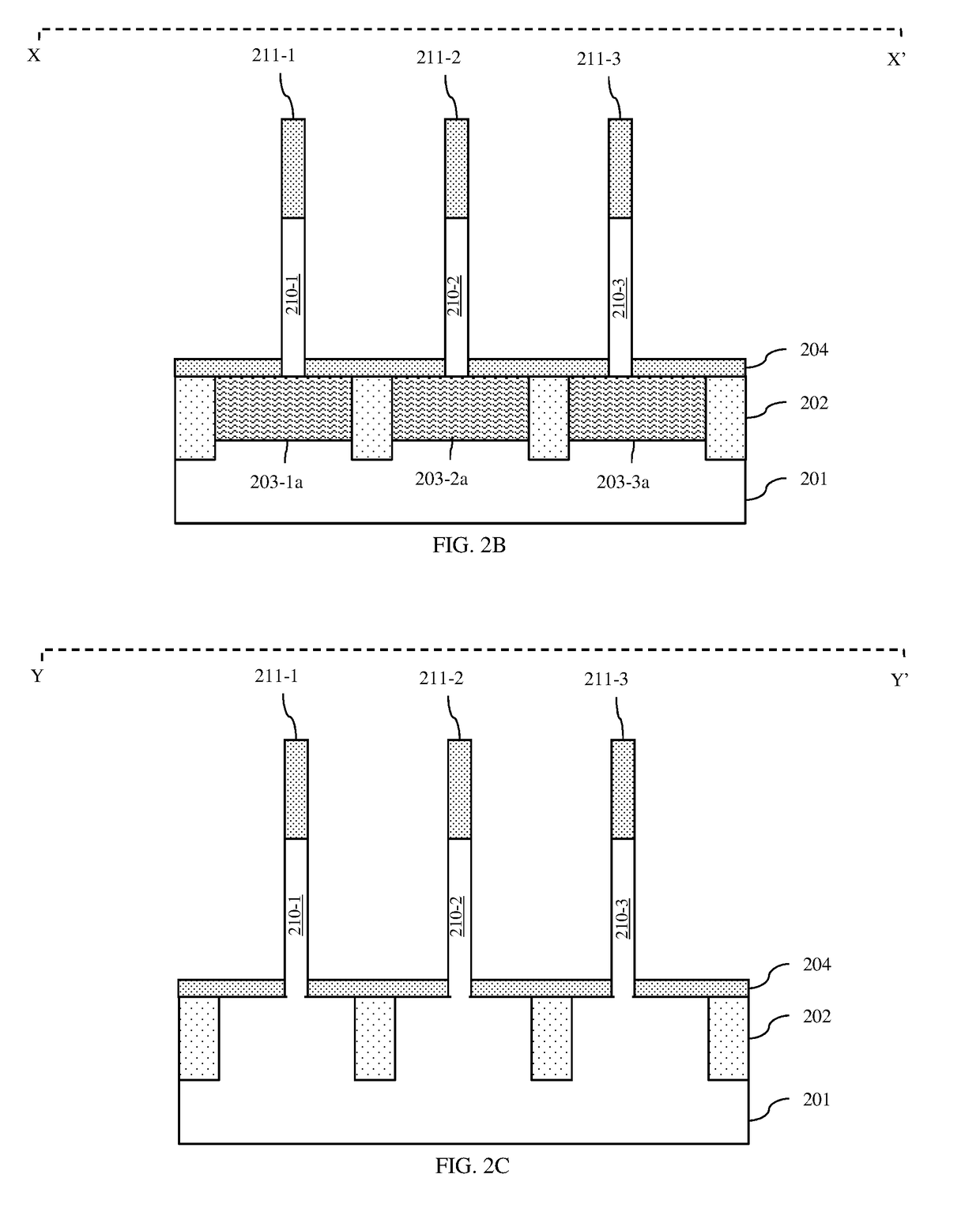
[0026]As mentioned above, as the device density (i.e., the number of devices per unit area) included in IC design specifications continues to be increased, forming the above-mentioned non-planar FETs without violating design rules and / or risking the formation of defects (e.g., shorts) can be difficult. For example, an IC design may include an array of vertical field effect transistors (VFETs) that incorporates a row of P-type VFETs adjacent to a row of N-type VFETs. With each new design generation, the specified fin pitch is reduced in order to increase VFET density within each row in the array and the reduction in fin pitch requires a corresponding reduction in the gate pitch in order to minimize parasitic capacitance. In VFETs, gate pitch reduction can be achieved through the formation of self-aligned gates. However, since the self-aligned gates are aligned below upper source / drain regions, gate extension(s) are required in order to provide a landing surface for gate contacts. In ...


PUM


Abstract

Disclosed is a method of forming an integrated circuit (IC) that incorporates multiple vertical field effect transistors (VFETs) (e.g., in a VFET array). In the method, self-aligned gates for each pair of VFETs and a self-aligned gate extension for contacting those self-aligned gates are essentially simultaneously formed such that the gates wrap around a pair of semiconductor fins, which are in end-to-end alignment, and such that the gate extension fills the space between adjacent ends of those semiconductor fins. By forming self-aligned gates and a self-aligned gate extension for a pair of VFETs, the method avoids the need for lithographically patterning extension cut isolation regions between adjacent pairs of VFETs in a VFET array. Thus, the method enables implementation of VFET array designs with a reduced fin pitch without incurring defects caused, for example, by overlay errors. Also disclosed herein is an IC formed according to the method.

Description

BACKGROUNDField of the Invention[0001]The present invention relates to vertical field effect transistors (VFETs) and, more particularly, to a method of forming multiple VFETs with self-aligned gates and gate extensions and the resulting integrated circuit (IC) structure.Description of Related Art[0002]Integrated circuit (IC) design decisions are often driven by device scalability, device density, device performance, manufacturing efficiency and costs. For example, IC designs may incorporate non-planar field effect transistor (FET) structures because non-planar FETs consume less chip surface area than planar FETs. Additionally, non-planar FETs exhibit multi-dimensional field effects as compared to the single-dimensional field effects exhibited by planar FETs and, thus, non-planar FETs exhibit improved gate control over the channel region. Exemplary non-planar FETs include, for example, standard fin-type FETs (FINFETs) and vertical fin-type FETs (VFETs). A FINFET is a non-planar FET t...

Claims


Application Information

Patent Timeline
IPC IPC(8): H01L29/66
CPCH01L29/66666H01L29/66545H01L29/6656H01L29/7827H01L29/4238
Inventor XIE, RUILONGLIEBMANN, LARSZANG, HUIBENTLEY, STEVEN
Owner GLOBALFOUNDRIES US INC
Why Eureka
Try Eureka