Method for forming multijunction metamorphic solar cells for space applications

a solar cell and multi-junction technology, applied in the field of solar cells and the fabrication of solar cells, can solve the problems of tens of more complex requirements for proper specification and manufacture, and achieve the effect of increasing the efficiency of photoconversion

Inactive Publication Date: 2019-03-21
SOLAERO TECH CORP
View PDF6 Cites 2 Cited by
  • Summary
  • Abstract
  • Description
  • Claims
  • Application Information

AI Technical Summary

Benefits of technology

[0015]It is an object of the present disclosure to provide increased photoconversion efficiency in a multijunction solar cell for space applications over the operational life of the photovoltaic power system.
[0016]It is another object of the present disclosure to provide in a multijunction solar cell in which the selection of the composition of the subcells and their band gaps maximizes the efficiency of the solar cell at a predetermined high temperature (in the range of 40 to 100 degrees Centigrade) in deployment in space at AM0 at a predetermined time after the initial deployment, such time being at least one year, and in the range of one to twenty-five years.

Problems solved by technology

Compared to silicon, III-V compound semiconductor multijunction devices have greater energy conversion efficiencies and generally more radiation resistance, although they tend to be more complex to properly specify and manufacture.

Method used


Image

  • Method for forming multijunction metamorphic solar cells for space applications
  • Method for forming multijunction metamorphic solar cells for space applications
  • Method for forming multijunction metamorphic solar cells for space applications

Examples


first embodiment

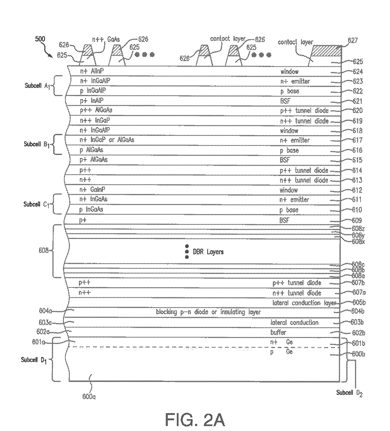
[0159]Turning to the fabrication of the multijunction solar cell assembly of the present disclosure, and in particular a five-junction solar cell assembly, FIG. 2A is a cross-sectional view of a semiconductor body 500 after several stages of fabrication including the growth of certain semiconductor layers on the growth substrate, and formation of grids and contacts on the contact layer of the top side (i.e., the light-facing side) of the semiconductor body.

[0160]As shown in the illustrated example of FIG. 2A, the bottom subcell (which we refer to initially as subcell D) includes a substrate 600 formed of p-type germanium (“Ge”) in some embodiments, which also serves as a base layer of the subcell (i.e., the p-polarity layer of a “base-emitter” photovoltaic junction formed by adjacent layers of opposite conductivity type).

[0161]In some embodiments, the bottom subcell D is germanium, while in other embodiments the fourth subcell is InGaAs, GaAsSb, InAsP, InAlAs, or SiGeSn, InGaAsN, In...

second embodiment

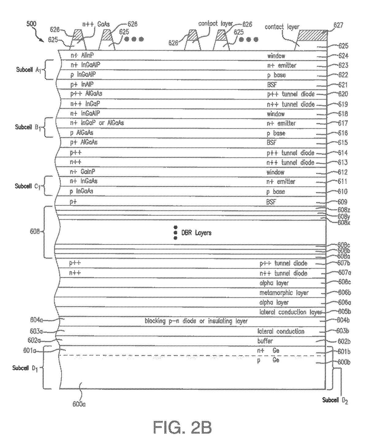
[0180]FIG. 2B is a cross-sectional view of a semiconductor body including a four solar subcells including two lattice mismatched subcells with a metamorphic layer between them, after several stages of fabrication including the growth of certain semiconductor layers on the growth substrate up to the contact layer, according to the present disclosure.

[0181]As shown in the previously illustrated example of FIG. 2A, the bottom subcell (which we refer to initially as subcell D) includes a substrate 600 formed of p-type germanium (“Ge”) in some embodiments, which also serves as a base layer, and since the layers 601 through 605 are substantially the same as described in connection with FIG. 2A, they will not be described in detail here for brevity.

[0182]In the embodiment of FIG. 2B, a first alpha layer 606a, composed of n-type (Al)GaIn(As)P, is deposited over the first lateral conduction layer 605, to a thickness of between 0.25 and 1.0 micron. Such an alpha layer is intended to prevent t...


PUM


Abstract

A method of manufacturing a multijunction solar cell including growing interconnected first and second discrete semiconductor regions disposed adjacent and parallel to each other in a single semiconductor body, including first top subcell, second (and possibly third) lattice matched middle subcells; a graded interlayer adjacent to the last middle solar subcell; and a bottom solar subcell adjacent to said graded interlayer being lattice mismatched with respect to the last middle solar subcell; wherein the interconnected regions form at least a four junction solar cell by a series connection being formed between the bottom solar subcell in the first semiconductor region and the bottom solar subcell in the second semiconductor region.

Description

REFERENCE TO RELATED APPLICATIONS[0001]This application is a division of U.S. patent application Ser. No. 15 / 250,643 filed Aug. 29, 2016.[0002]The Ser. No. 15 / 250,643 application claims the benefit of U.S. Provisional Application No. 62 / 288,181 filed Jan. 28, 2016, and U.S. Provisional Patent Application Ser. No. 62 / 243,239 filed Oct. 19, 2015.[0003]This application is related to co-pending U.S. patent application Ser. Nos. 14 / 828,197 and 14 / 828,206 filed Aug. 17, 2015; Ser. No. 15 / 210,532 filed Jul. 14, 2016; and Ser. No. 15 / 213,594 filed Jul. 19, 2016, and Ser. No. 15 / 250,673, now U.S. Pat. No. ______ filed Aug. 29, 2016.[0004]This application is also related to co-pending U.S. patent application Ser. No. 14 / 660,092 filed Mar. 17, 2015, which is a division of U.S. patent application Ser. No. 12 / 716,814 filed Mar. 3, 2010, now U.S. Pat. No. 9,018,521; which was a continuation in part of U.S. patent application Ser. No. 12 / 337,043 filed Dec. 17, 2008.[0005]This application is also r...

Claims


Application Information

Patent Timeline
Patent Type & Authority Applications(United States)
IPC IPC(8): H01L31/0725H01L31/0735H01L31/054H01L31/18H01L31/02H01L31/0304H01L31/078H01L31/05H01L31/0687
CPCY02E10/52Y02E10/544H01L31/078H01L31/0687H01L31/0504H01L31/0725H01L31/02008H01L31/1844H01L31/0547H01L31/0735H01L31/03046
Inventor DERKACS, DANIEL
Owner SOLAERO TECH CORP
Why Eureka
Try Eureka