Organic light emitting display device and method for driving the same

a display device and organic technology, applied in semiconductor devices, instruments, electrical apparatuses, etc., can solve the problems of image quality deterioration, and reduced life of the element, so as to suppress ripple in the initialization power supply, suppress stains or blemishes, and remove luminance deviations.

Active Publication Date: 2019-03-28
LG DISPLAY CO LTD
View PDF11 Cites 10 Cited by
  • Summary
  • Abstract
  • Description
  • Claims
  • Application Information

AI Technical Summary

Benefits of technology

[0032]The organic light-emitting display device according to one embodiment of the present disclosure includes the transistor for initializing the node between the driving transistor and the capacitor to the reference voltage for an initialization period. In this connection, the transistor is turned on based on the signal (i−1)-th scan signal corresponding to the previous scan-line. This prevents a short circuit from occurring between the in

Problems solved by technology

In this instance, as the driving current is reduced due to the variation of the threshold voltage of the driving element, an image quality is deteriorated and the lifetime of the element is reduced.
Thus, a ripple may occur in the initialization power supply.
Due to the ripple in the initi

Method used


Image

  • Organic light emitting display device and method for driving the same
  • Organic light emitting display device and method for driving the same
  • Organic light emitting display device and method for driving the same

Examples


first embodiment

[0048]First, an organic light-emitting display device according to the present disclosure and a method for driving the device will be described with reference to FIGS. 1 to 3.

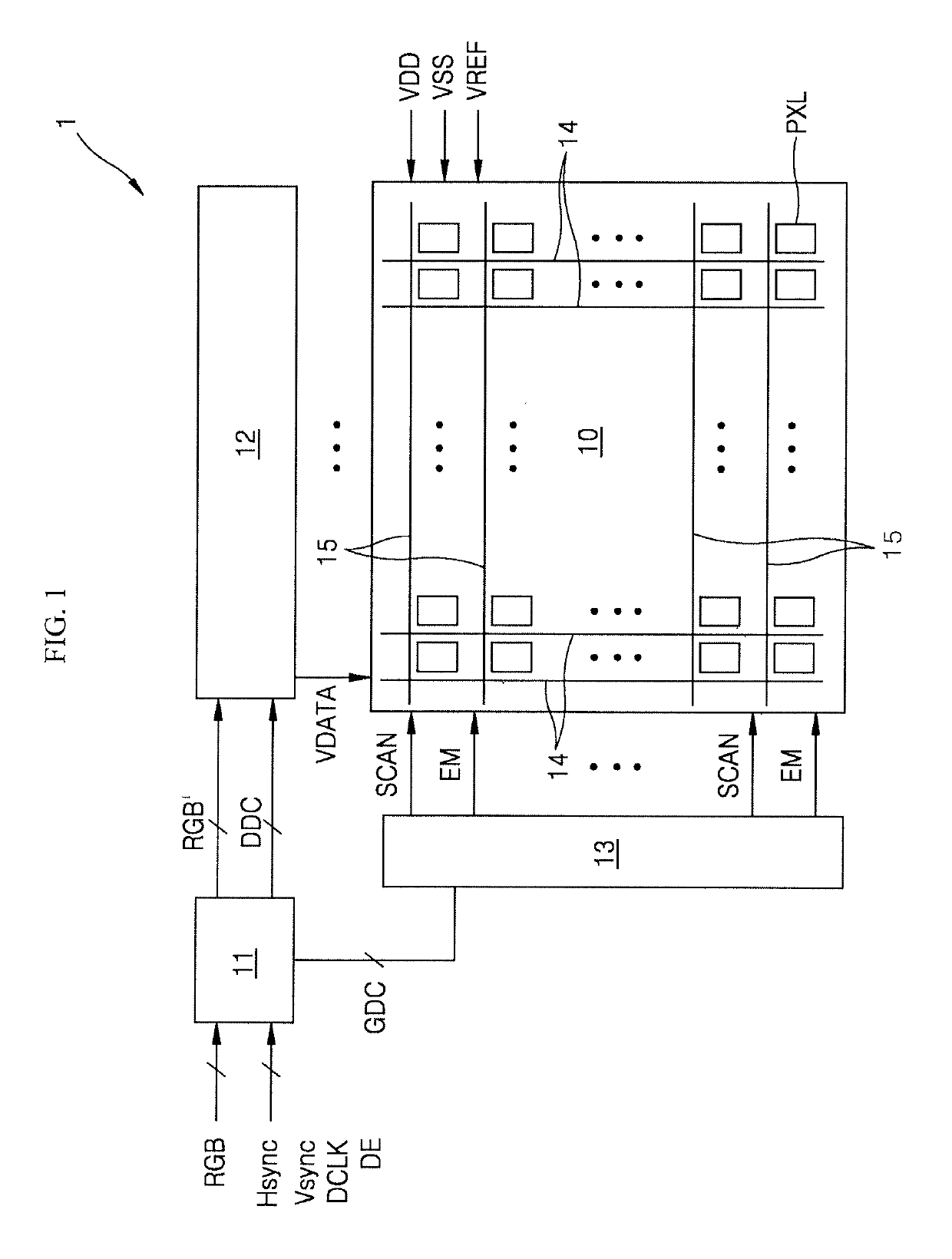
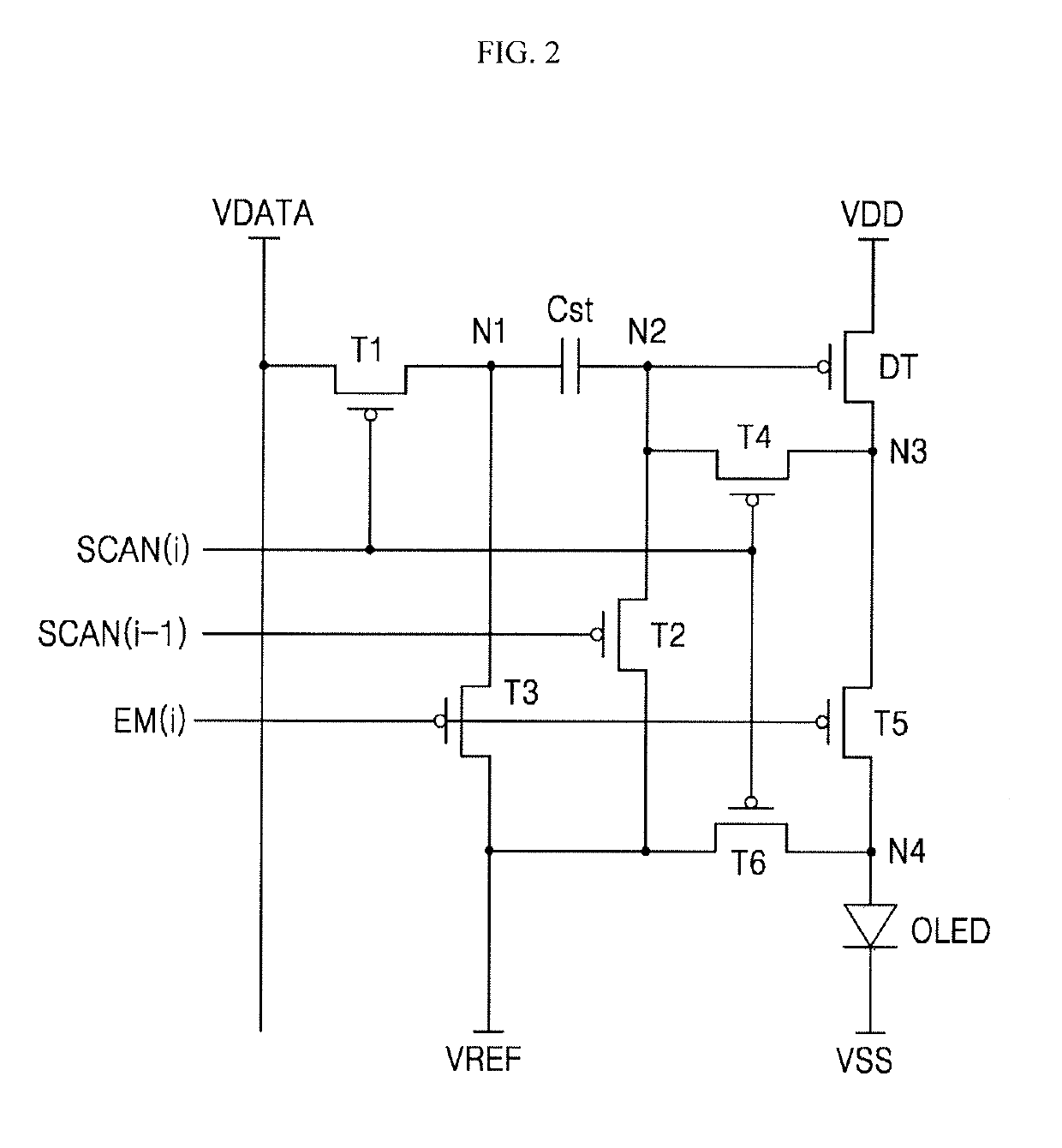
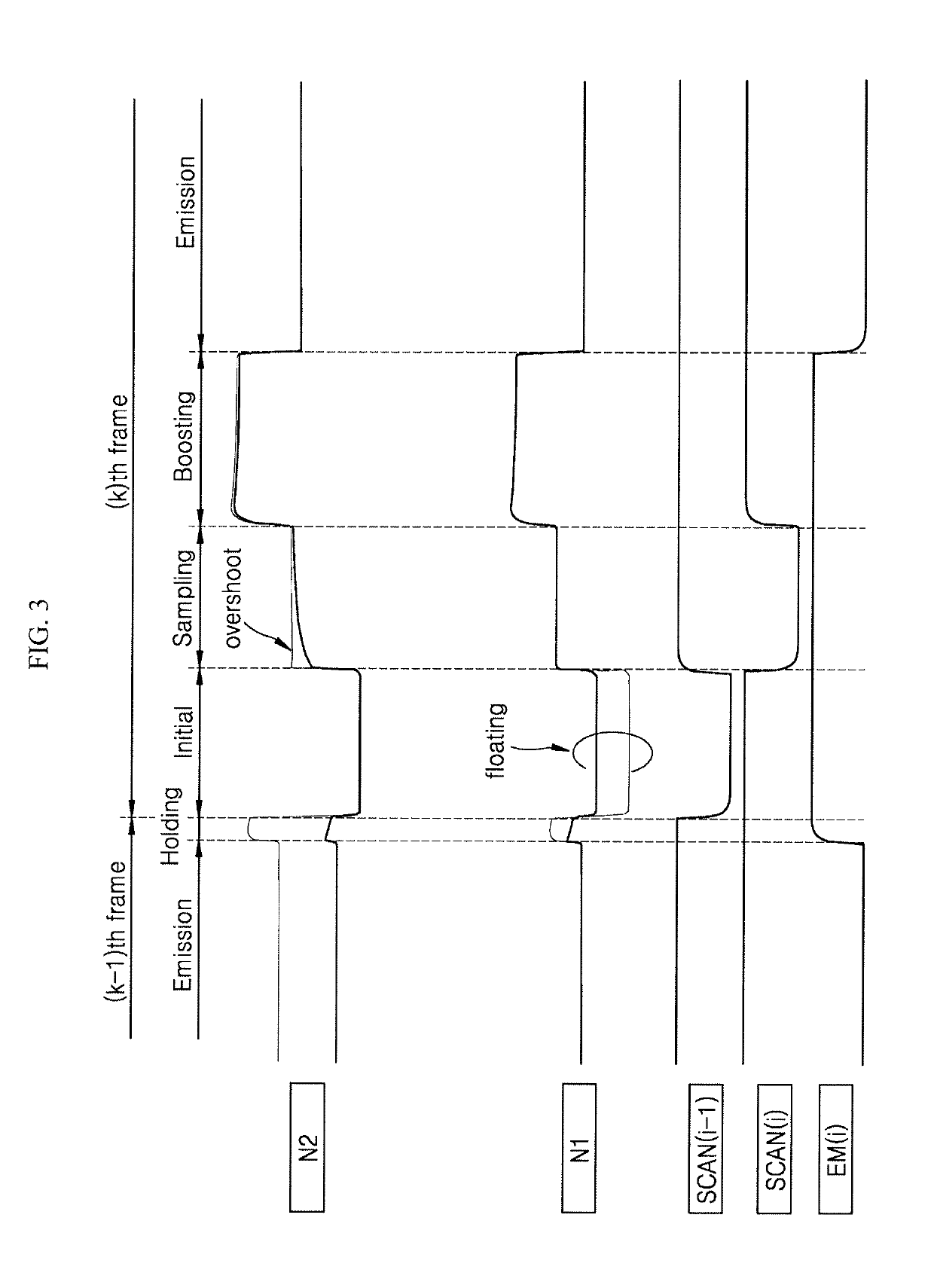
[0049]FIG. 1 illustrates an organic light-emitting display device according to a first embodiment of the present disclosure. FIG. 2 shows an equivalent circuit corresponding to any one pixel in an organic light-emitting display device according to the first embodiment of the present disclosure. FIG. 3 shows a waveform of a driving signal in FIG. 2 and an associated potential at each node.

[0050]As illustrated in FIG. 1, an organic light-emitting display device 1 according to a first embodiment of the present disclosure includes a display panel 10 including a plurality of pixel PXLs, a data driving circuit 12 for driving data-lines 14 of the display panel 10, a gate driving circuit 13 for driving scan-lines 15 of the display panel 10, and a timing controller 11 for controlling the driving timing of the data drivi...

second embodiment

[0108]To solve this problem, in accordance with the present disclosure, a second embodiment is provided in which both potentials of the first and second nodes N1 and N2 are initialized for the initialization period (Initial).

[0109]FIG. 4 shows an equivalent circuit corresponding to any one pixel in an organic light-emitting display device according to the second embodiment of the present disclosure. FIG. 5 shows a waveform of a driving signal in FIG. 4 and an associated potential at each node according to the second embodiment of the present disclosure.

[0110]As illustrated in FIG. 4, the organic light-emitting display device according to the second embodiment of the present disclosure further includes a seventh transistor T7. When the seventh transistor T7 is turned on based on the (i−1)-th scan signal SCAN(i−1), the reference voltage VREF is supplied to the first node N1 via the turned-on seventh transistor T7. Except for the presence of the seventh transistor T7, a configuration o...

third embodiment

[0118]FIG. 6 shows an equivalent circuit corresponding to any one pixel in an organic light-emitting display device according to the present disclosure.

[0119]As illustrated in FIG. 6, in the organic light-emitting display device according to the third embodiment of the present disclosure, when the second transistor T2 turns on, a first reference voltage VREF1 is supplied to the second node N2 via the turned-on second transistor T2. At the same time, when the seventh transistor T7 turns on, the first node N1 is supplied with a second reference voltage VREF2 which is different from the first reference voltage VREF1. A configuration of the third embodiment is the same as those of the first and second embodiments illustrated in FIGS. 1 to 5, except that, in the third embodiment, the first reference voltage for initializing the first node N1 and the second reference voltage for initializing the second node N2 have different voltage levels. Therefore, the descriptions of the overlapping p...


PUM


Abstract

An organic light-emitting display device can include an organic light-emitting element; a driving transistor connected in series with the organic light-emitting element, the driving transistor and the organic light-emitting element being between a first driving power supply line for supplying a first driving voltage and a second driving power supply line for supplying a second driving voltage lower than first driving voltage; a first transistor configured to turn on based on an i-th scan signal and supply a data voltage to a first node, where i is a natural number greater than or equal to 2 and less than or equal to N, and N is a number of scan-lines; a capacitor between the first node and a gate electrode of the driving transistor, the capacitor is configured to supply a turn-on signal of the driving transistor to the gate electrode of the driving transistor based on the data voltage; and a second transistor configured to turn on based on a (i−1)-th scan signal and supply a first reference voltage to a second node, in which the second node is disposed between the driving transistor and the capacitor, and the capacitor is between the first and second nodes.

Description

CROSS-REFERENCE TO RELATED APPLICATION[0001]This application claims priority to and the benefit of Korean Patent Application No. 10-2017-0126235, filed in the Republic of Korea on Sep. 28, 2017, the disclosure of which is incorporated herein by reference in its entirety.BACKGROUNDTechnical Field[0002]The present disclosure relates to an active-matrix scheme-based organic light-emitting display device including a compensation circuit, and a method for driving the same.Related Art[0003]A display device applies to a variety of electronic devices, such as TVs, mobile phones, notebooks and tablets. Therefore, studies are being continued to develop thinner, lighter and lower-power consuming display devices.[0004]A typical example of the display device may include a liquid crystal display device (LCD), a plasma display panel device (PDP), a field emission display device (FED), an electro luminescence display device (ELD), an electro-wetting display device (EWD) and, an organic light-emitti...

Claims


Application Information

Patent Timeline
IPC IPC(8): G09G3/3291H01L27/32G09G3/3266
CPCG09G2300/043G09G2310/08G09G2300/0426G09G3/3291H01L27/3244G09G3/3266G09G3/3208G09G3/3233G09G3/3258G09G2300/0819G09G2300/0861G09G2310/0262G09G2310/061G09G2320/043G09G2320/0233G09G2300/0842G09G2230/00H10K59/12
Inventor LEE, TAEKYEONG
Owner LG DISPLAY CO LTD
Why Eureka
Try Eureka