

Solid-state imaging device and electronic device
a solid-state imaging and electronic device technology, applied in the direction of semiconductor devices, radio frequency controlled devices, electrical devices, etc., can solve the problem of not having a technology method established, and achieve the effect of expanding the dynamic range of pixel including the high-sensitivity pixel and the low-sensitivity pixel
Active Publication Date: 2019-03-28
SONY CORP
View PDF4 Cites 15 Cited by
- Summary
- Abstract
- Description
- Claims
- Application Information
AI Technical Summary
Benefits of technology
The patent expands the dynamic range of pixels in a camera sensor. This includes both high-sensitivity and low-sensitivity pixels. The effect of this is that the camera can capture more detail in both bright and dark areas, improving image quality.
Problems solved by technology
By the way, to expand the dynamic range using a difference in sensitivity between the high-sensitivity pixel and the low-sensitivity pixel, further expansion of the dynamic range is required, but at present, such a technology method has not been established yet.
Method used
View moreImage
Smart ImageViewing Examples

Examples
first embodiment
[0070]2. Structure Including Overflow Path in Pixel
second embodiment
[0071]3. Structure Having Limited Size in Depth Direction of Low-Sensitivity PD
third embodiment
[0072]4. Structure Having Different Sizes in Plane Direction on Incident Light Side and on Wiring Side of Low-Sensitivity PD
Login to View More PUM
 Abstract
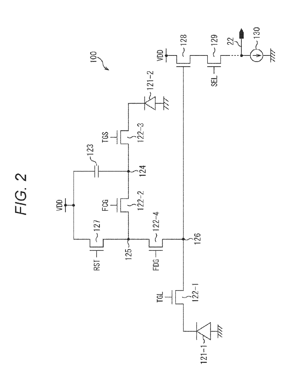
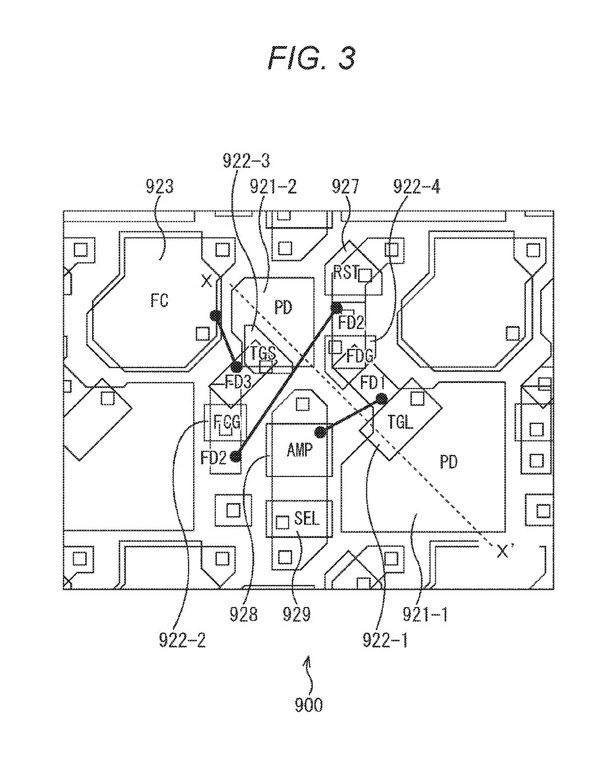
The present technology relates to a solid-state imaging device and an electronic device that can expand a dynamic range in a pixel having a high-sensitivity pixel and a low-sensitivity pixel. The solid-state imaging device includes a pixel array unit in which a plurality of pixels is arranged in a two-dimensional manner, in which the pixel includes a first photoelectric conversion unit and a second photoelectric conversion unit having lower sensitivity than the first photoelectric conversion unit, and a size of the second photoelectric conversion unit in an optical axis direction in which light enters is smaller than a size of the first photoelectric conversion unit in the optical axis direction. The present technology can be applied to a backside-illumination CMOS image sensor, for example.
Description
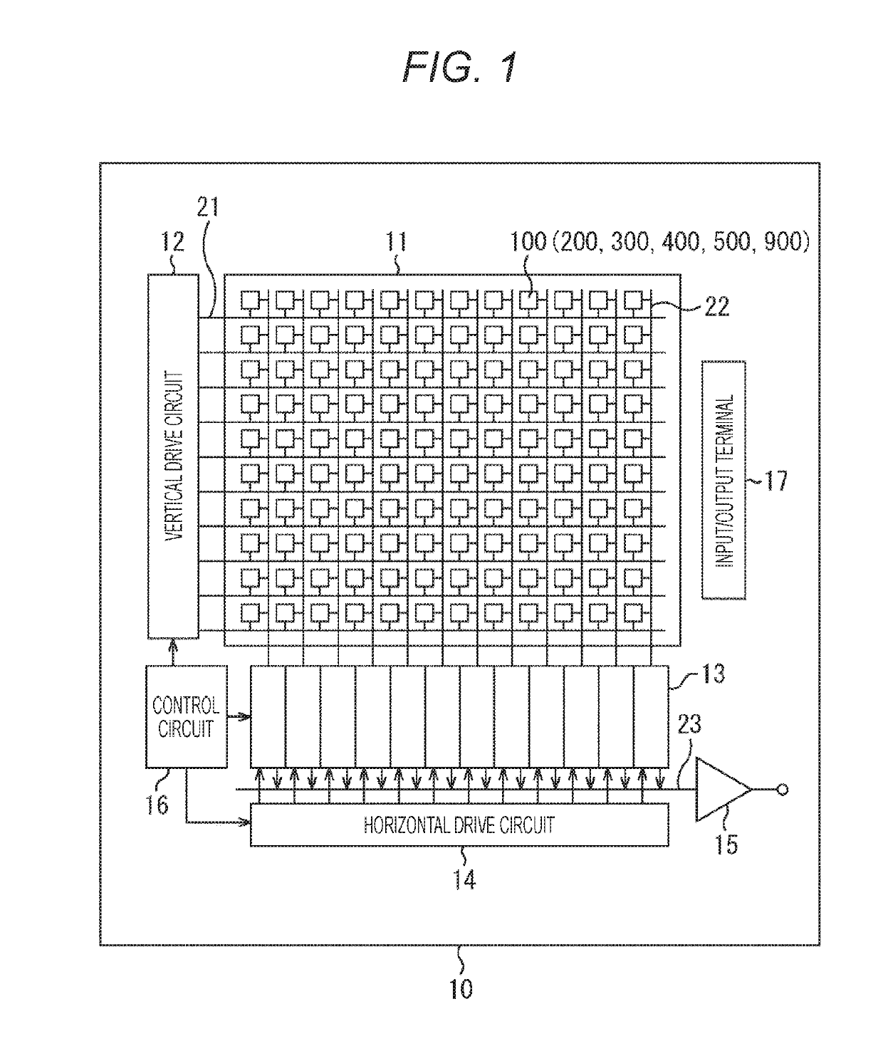
TECHNICAL FIELD[0001]The present technology relates to a solid-state imaging device and an electronic device, and in particular to a solid-state imaging device and an electronic device that can expand a dynamic range in a pixel including a high-sensitivity pixel and a low-sensitivity pixel.BACKGROUND ART[0002]A solid-state imaging device such as a complementary metal oxide semiconductor (CMOS) image sensor is used in an electronic device such as an imaging device such as a digital still camera or a video camera, or a mobile terminal device having an imaging function, for example.[0003]The CMOS image sensor desirably has high sensitivity so that an imaging signal can be acquired at low illuminance. Furthermore, a photodiode is desirably less easily saturated so that the dynamic range becomes large. However, the sensitivity being high and the photodiode being less easily saturated are in a trade-off relationship, and expanding the dynamic range while maintaining the sensitivity is dif...
Claims
Login to View More Application Information
Patent Timeline
 IPC IPC(8): H01L27/146
CPCH01L27/14607H01L27/14645H01L27/14609H01L27/14616H01L27/14623H01L27/14627H01L27/1463H01L27/1464H01L27/14605H01L27/1461H01L27/14614H01L27/14638H01L27/14641H04N25/585H04N25/621H04N25/70
InventorKIDO, HIDEOTADA, MASAHIROTOYOSHIMA, TAKAHIROTATESHITA, YASUSHIIWATA, HIKARU
OwnerSONY CORP