
Polishing apparatus

Pending Publication Date: 2019-04-04
DISCO CORP
View PDF1 Cites 1 Cited by
  • Summary
  • Abstract
  • Description
  • Claims
  • Application Information

AI Technical Summary

Benefits of technology

The present invention provides a polishing apparatus that can effectively polish a wafer without causing edge chipping even on a thin wafer. This is achieved by a polishing pad with grooves on its adhesion surface and a flat polishing surface, which prevents collisions between angular parts and the wafer. The polishing liquid is distributed throughout the pad through the grooves, and it is further supplied to the polishing surface through communication holes, resulting in efficient polishing and prevention of edge chipping.

Problems solved by technology

However, angular parts between groove side surfaces and the polishing surface collide on an outer peripheral edge of the semiconductor wafer repeatedly, whereby a load is exerted on the outer peripheral edge, and, in the case of a thin semiconductor wafer, edge chipping may be generated.

Method used


Image

  • Polishing apparatus
  • Polishing apparatus
  • Polishing apparatus

Examples


Embodiment Construction

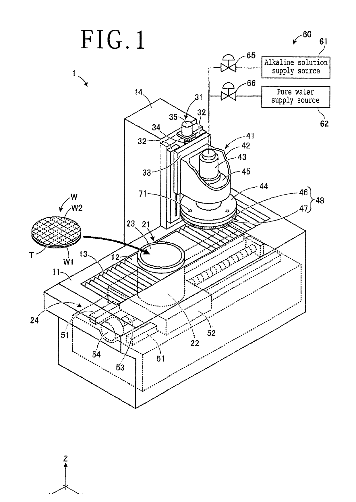
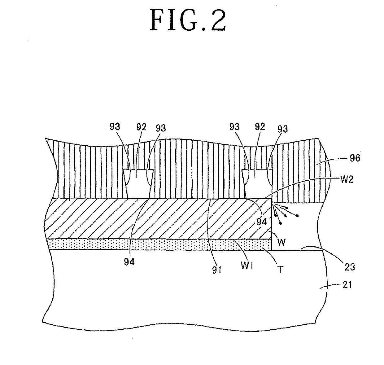
[0020]A polishing apparatus will be described below, referring to the attached drawings. FIG. 1 is a perspective view of a polishing apparatus according to the present embodiment. FIG. 2 is an illustration of polishing by a polishing pad formed with grooves in a polishing surface. Note that the polishing apparatus according to the present embodiment is not limited to the one as depicted in FIG. 1, and may be mounted in a full automatic type processing apparatus by which a series of processings such as grinding, polishing and cleaning are performed fully automatically.

[0021]As illustrated in FIG. 1, the polishing apparatus 1 is configured to polish a wafer W by chemical mechanical polishing (CMP) by use of a polishing pad 47 which will be described later. The wafer W is a silicon wafer, in which a plurality of streets are formed in a grid pattern on a front surface W1, and devices (not depicted) such as integrated circuits (ICs) and large-scale integrations (LSIs) are formed in regio...


PUM


Abstract

A polishing pad of a polishing apparatus contains abrasive grains, and is formed with a plurality of grooves in an adhesion surface to be adhered to a support base. The polishing pad has a plurality of communication holes penetrating to a flat polishing surface, and a polishing liquid is distributed into the plurality of grooves and is supplied to the polishing surface through the plurality of communication holes.

Description

BACKGROUND OF THE INVENTIONField of the Invention[0001]The present invention relates to a polishing apparatus for polishing a wafer.Description of the Related Art[0002]In the semiconductor device manufacturing step, a semiconductor wafer formed with a plurality of devices is divided along streets, to form semiconductor devices. For realizing reductions in size and weight of semiconductor devices, the back surface of the semiconductor wafer is ground before dividing the semiconductor wafer. When the semiconductor wafer is thus ground, a grinding strain layer composed of microcracks which is approximately 1 μm in thickness is formed on the back surface of the semiconductor wafer. When the thickness of the semiconductor wafer is reduced to or below 100 μm, the grinding strain layer reduces the die strength of the semiconductor devices.[0003]In order to solve such a problem, after the semiconductor wafer is ground to a predetermined thickness, the back surface of the semiconductor wafer...

Claims


Application Information

Patent Timeline
IPC IPC(8): B24B37/10B24B37/22H01L21/306
CPCB24B37/107B24B37/22H01L21/30625B24B37/044B24B37/105B24B37/26B24B57/02B24B37/04H01L21/304
Inventor ARIFUKU, NORIHISASARUMIDA, MAKOTO
Owner DISCO CORP
Features
  • Generate Ideas
  • Intellectual Property
  • Life Sciences
  • Materials
  • Tech Scout
  • Unparalleled Data Quality
  • Higher Quality Content
  • 60% Fewer Hallucinations
Learn More