Method of processing a substrate and a device manufactured by the same

a technology of substrate and processing method, which is applied in the direction of semiconductor devices, basic electric elements, electrical equipment, etc., can solve problems such as electrical short circuits, and achieve the effects of preventing excessive etching and improving the resistance of upper and lower surfaces

Active Publication Date: 2019-05-16
ASM IP HLDG BV
View PDF2 Cites 255 Cited by
  • Summary
  • Abstract
  • Description
  • Claims
  • Application Information

AI Technical Summary

Benefits of technology

[0008]One or more embodiments of the present disclosure are to prevent excessive etching in a part of the structure having steps, while forming a barrier layer.
[0009]One or more embodiments of the present disclosure are to improve resistance of upper and lower surfaces to wet-etching, in a stair-case

Problems solved by technology

However, when the via contact hole is formed, the via contact hole may be connected to another second insulating layer in the stair-case structure aft

Method used


Image

  • Method of processing a substrate and a device manufactured by the same
  • Method of processing a substrate and a device manufactured by the same
  • Method of processing a substrate and a device manufactured by the same

Examples


Embodiment Construction

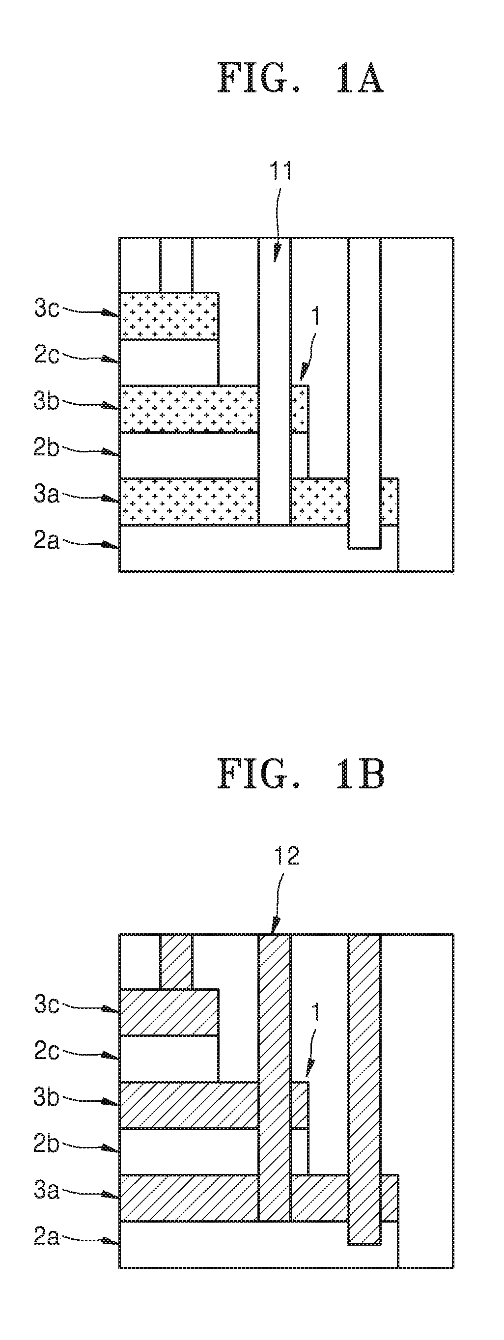
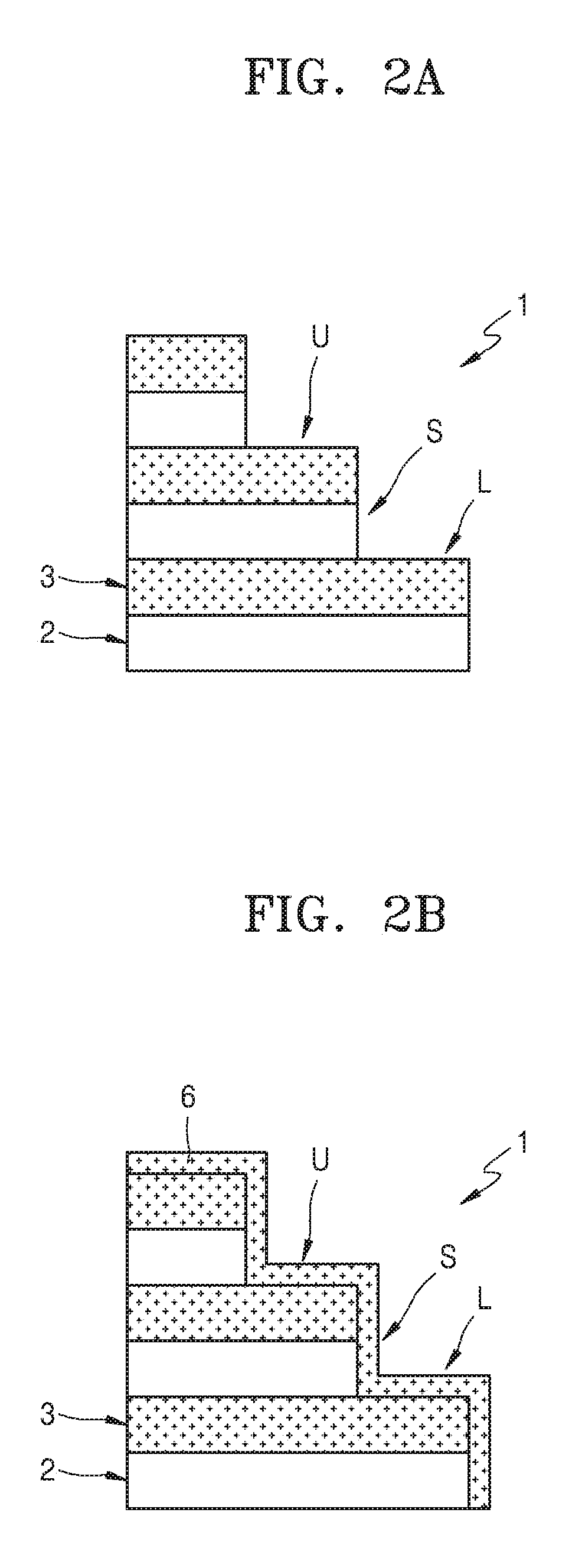
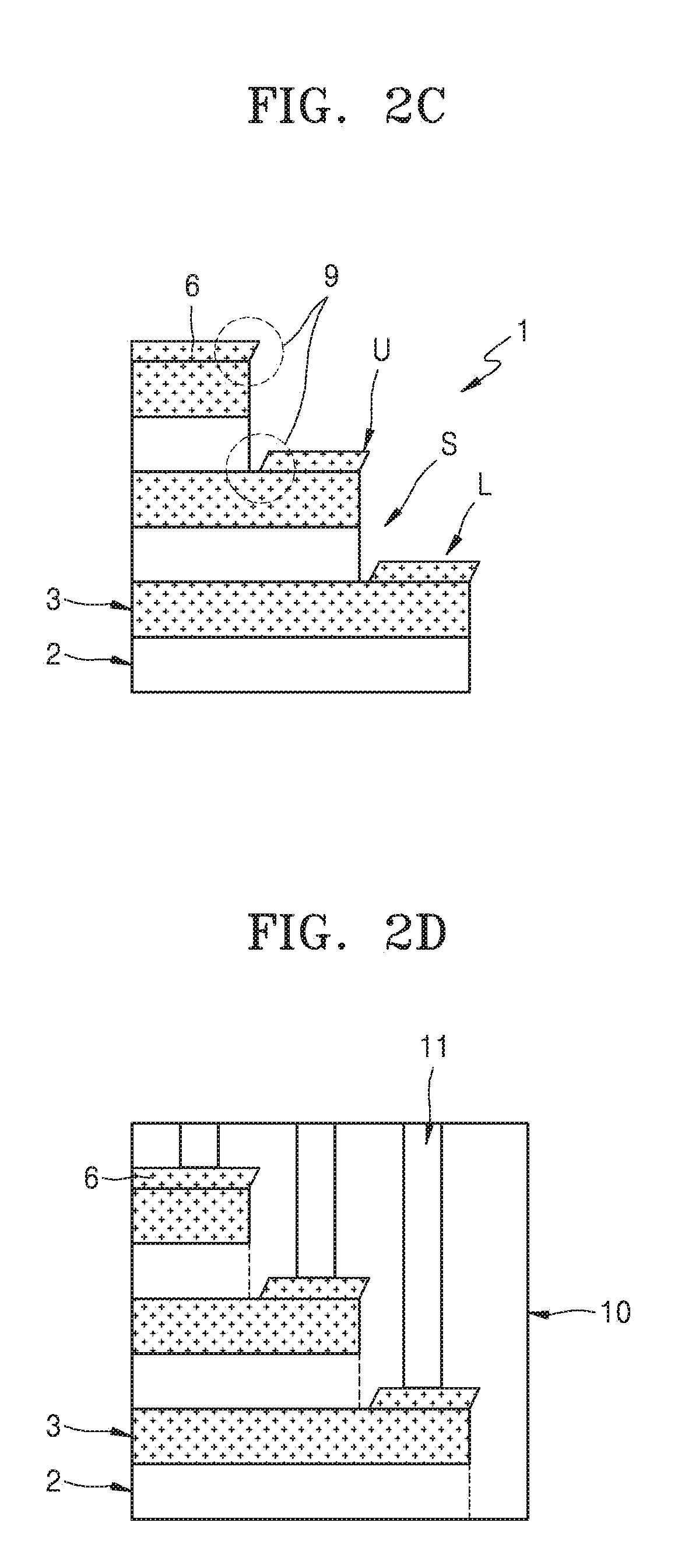
[0043]Reference will now be made in detail to embodiments, examples of which are illustrated in the accompanying drawings, wherein like reference numerals refer to like elements throughout. In this regard, the present embodiments may have different forms and should not be construed as being limited to the descriptions set forth herein. Accordingly, the embodiments are merely described below, by referring to the figures, to explain aspects of the present description. As used herein, the term “and / or” includes any and all combinations of one or more of the associated listed items. Expressions such as “at least one of,” when preceding a list of elements, modify the entire list of elements and do not modify the individual elements of the list.

[0044]Hereinafter, one or more embodiments of the present disclosure will be described in detail with reference to accompanying drawings.

[0045]Embodiments of the present disclosure are offered to illustrate more fully aspects of the present disclos...


PUM


Abstract

Provided is a substrate processing method capable of preventing over-etching of a part of a stair-case structure due to an etching solution, when a barrier layer is selectively formed on a VNAND device having the stair-case structure. The substrate processing method includes: alternately stacking a first insulating layer and a second insulating layer; forming a stepped structure having an upper surface, a lower surface, and a side surface connecting the upper surface to the lower surface by etching the first insulating layer and the second insulating layer that are stacked; densifying the stepped structure; forming a barrier layer on the densified second insulating layer; and performing isotropic etching on at least a part of a sacrificial word line structure including the second insulating layer and the barrier layer. During etching the barrier layer at the isotropic etching step, the second insulating layer is not etched or etched a little to an ignorable degree.

Description

CROSS-REFERENCE TO RELATED APPLICATION[0001]This application claims the benefit of Korean Patent Application No. 10-2017-0153314, filed on Nov. 16, 2017, in the Korean Intellectual Property Office, the disclosure of which is incorporated herein in its entirety by reference.BACKGROUND1. Field[0002]One or more embodiments relate to a substrate processing method using a thin film deposition technique and a device manufactured by the method, and more particularly, to a method of processing a substrate by depositing an insulating layer (e.g., a silicon nitride layer) on a substrate by a plasma-enhanced atomic layer deposition (PEALD) method and a device manufactured by the method (e.g., a semiconductor device).2. Description of the Related Art[0003]Recently, demand for three-dimensional (3D) vertical NAND (VNAND) flash devices has been rapidly increasing. In order to process more information, the number of times that a first insulating layer and a second insulating layer of a stack gate ...

Claims


Application Information

Patent Timeline
IPC IPC(8): H01L27/11582H01L27/11556H01L21/822H01L21/311
CPCH01L27/11582H01L27/11556H01L21/8221H01L21/31116H01L21/3105H01L21/0217H01L21/02274H01L21/0228H01L21/0234H01L21/02219H01L21/31111H10B41/50H10B43/50H10B41/41H10B41/35H10B41/20H01L21/31127H01L21/311H01L21/31105H10B41/27H10B43/27
Inventor KIM, YOUNG HOONCHOI, JONG WANWOO, JEONG JUNYOO, TAE HEE
Owner ASM IP HLDG BV
Why Eureka
Try Eureka