Semiconductor device having a structure to improve contact processing margin, and method of fabricating the same

a technology of semiconductor devices and processing margins, which is applied in the field of semiconductor devices, can solve the problems of insufficient processing margins, reduced performance and/or yield of semiconductor devices, and excessive etching of a lower conductive layer, and achieve the effect of preventing excessive etching of a conductive layer

Inactive Publication Date: 2007-02-15
DONGBU ELECTRONICS CO LTD +1
View PDF2 Cites 0 Cited by
  • Summary
  • Abstract
  • Description
  • Claims
  • Application Information

AI Technical Summary

Benefits of technology

[0010] It is, therefore, an object of the present invention to obtain processing margin and prevent excessive etching of a conductive layer under a salicide, even if misalignment of an overlying contact hole happens.

Problems solved by technology

A short interval between a contact and a non-salicide region may cause insufficient processing margin when fabricating a semiconductor device, including SRAM devices.
Misalignment resulting from the insufficient processing margin at a contact forming step may cause excessive etching of a lower conductive layer.
Such excessive etching of a conductive layer may adversely affect a leakage current property so that performance and / or yield of a semiconductor device may decrease.
A short distance “A” between the second contact 82 and the non-salicide region 51 may cause a serious problem when misalignment happens at a contact etching step.
As a result, it can be seen that excessive etching of a conductive layer adversely affects a leakage current property of the device so that performance and / or yield of the device drops.

Method used


Image

  • Semiconductor device having a structure to improve contact processing margin, and method of fabricating the same
  • Semiconductor device having a structure to improve contact processing margin, and method of fabricating the same
  • Semiconductor device having a structure to improve contact processing margin, and method of fabricating the same

Examples


Embodiment Construction

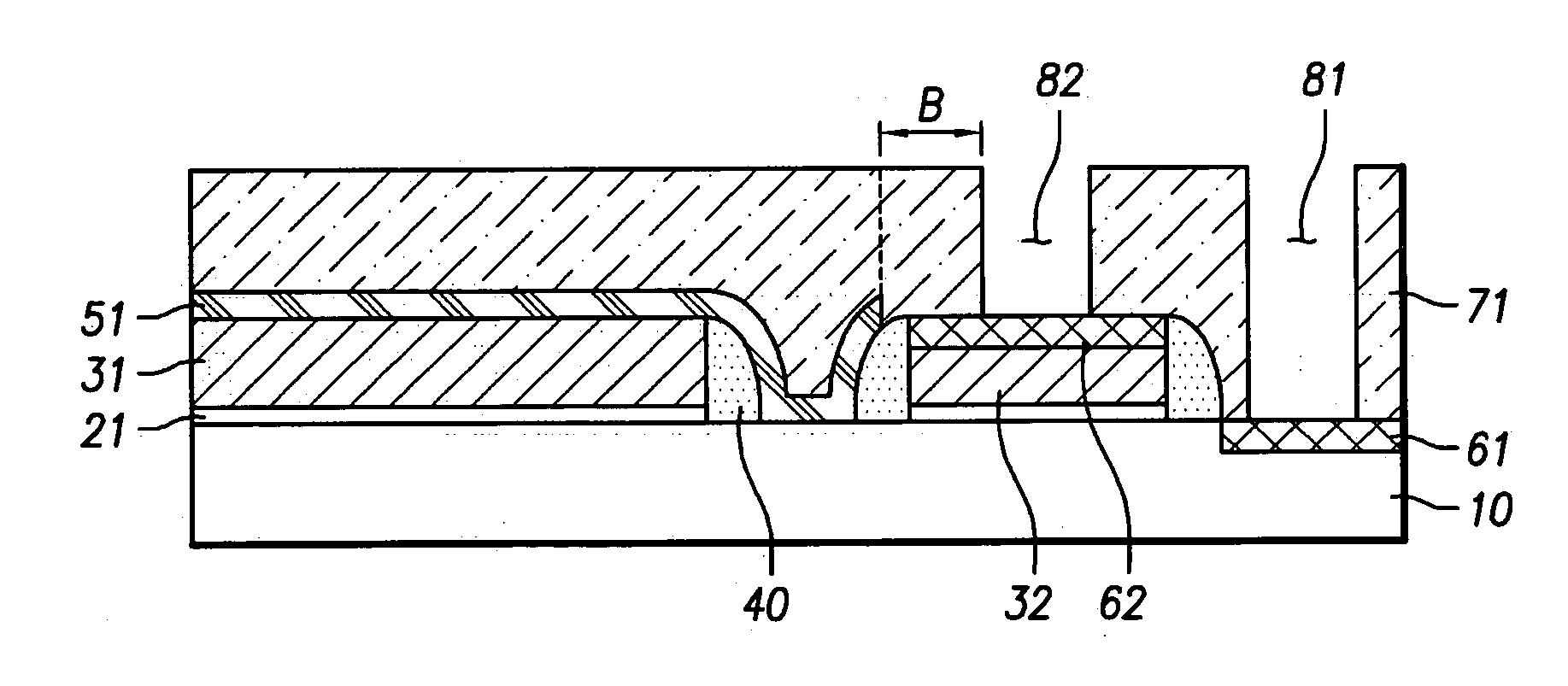
[0023] To clarify the present invention, techniques known widely to the corresponding technical filed and not directly related to the present invention are not shown in this description. Some components are omitted, exaggerated or proximately illustrated in the accompanying drawings for the same reason, and thus, a component's size as shown in the accompanying Figures does not always reflect reality.

[0024]FIG. 4 shows a part of layout of a semiconductor device (1T-SRAM) according to an embodiment of the present invention. Parts of the semiconductor device layout are common in FIG. 4 and FIG. 1, so that reference numbers used in FIG. 4 correspond to those in FIG. 1. As shown in FIG. 4, an interval or distance (“B”) between the non-salicide region 51 and the second contact 82 connecting to the second conductive pattern 32 is sufficient to perform a following process and provide sufficient or adequate processing margin at a contact-etching step. It is preferable that the interval (B) ...


PUM

PropertyMeasurementUnit
distanceaaaaaaaaaa
insulatingaaaaaaaaaa
conductiveaaaaaaaaaa

Abstract

A method for fabricating a semiconductor device includes forming a first insulating pattern, a first conductive pattern, and a second conductive pattern on a semiconductor substrate; forming a spacer on sidewalls of the first insulating pattern, the first conductive pattern, and the second conductive pattern; forming a second insulating pattern over the substrate; forming a first salicide on an exposed portion of the substrate and a second salicide on an entire upper surface of the second conductive pattern; depositing a third insulating layer over the substrate, and etching selectively the third insulating layer to forming first and second contact holes exposing the first and second salicides. The method provides processing margin and prevents excessive etching of a conductive layer under the salicide, even if misalignment of an overlying contact hole happens.

Description

[0001] This application claims the benefit of Korean Application No. 10-2005-0074210, filed on Aug. 12, 2005, which is incorporated by reference herein in its entirety. BACKGROUND OF THE INVENTION [0002] 1. Field of the Invention [0003] The present invention relates to a semiconductor device and a fabrication method thereof, and more specifically, to a semiconductor device having a structure to improve contact processing margin and a method for fabricating the same. [0004] 2. Description of the Related Art [0005] A short interval between a contact and a non-salicide region may cause insufficient processing margin when fabricating a semiconductor device, including SRAM devices. Misalignment resulting from the insufficient processing margin at a contact forming step may cause excessive etching of a lower conductive layer. Such excessive etching of a conductive layer may adversely affect a leakage current property so that performance and / or yield of a semiconductor device may decrease....

Claims


Application Information

Patent Timeline
Patent Type & Authority Applications(United States)
IPC IPC(8): H01L21/336
CPCH01L27/11H01L21/76897H10B10/00H01L21/28H01L21/24
Inventor KIM, DAE KYEUNPARK, JEONG HO
Owner DONGBU ELECTRONICS CO LTD
Why Eureka
Try Eureka