Semiconductor device and semiconductor device manufacturing method

a semiconductor device and semiconductor technology, applied in semiconductor devices, semiconductor/solid-state device testing/measurement, semiconductor/solid-state device details, etc., can solve the problems of excessive etching of the cu film included in the redistribution, reduced resistance, au film peeling,

Active Publication Date: 2019-05-02
LAPIS SEMICON CO LTD
View PDF2 Cites 0 Cited by
  • Summary
  • Abstract
  • Description
  • Claims
  • Application Information

AI Technical Summary

Benefits of technology

[0009]The present disclosure provides a semiconductor device that may prevent excessive etching of a conductive member included in a redistribution due to a local cell effect.
[0012]According to the above aspects, the present disclosure provides a semiconductor device that may prevent a conductive member included in a redistribution from being excessively etched due to a local cell effect.

Problems solved by technology

Redistribution with a laminated film including a Cu film and an Au film not only reduces resistance, but also prevents oxidation of the Cu film in manufacturing processes.
In the present discloser, in a case in which a redistribution is made with a laminated film including a Cu film and an Au film, the Au film and the Cu film generate a local cell effect in an etching process to remove a seed layer, causing excessive etching of the Cu film included in the redistribution.
In a case where a wire in the redistribution has a small width, excessive etching of the Cu film due to the local cell effect may vanishe the Cu film completely, which may cause peeling of the Au film.
Further, even in a case in which the Cu film does not completely vanish, excessive etching of the Cu film reduces a contact area between the Cu film and an insulating film (serving as a base of the redistribution), which reduces adhesion of the redistribution with respect to the insulating film.
Furthermore, since the Au film covers the excessively etched Cu film like an eave, observing and checking the state of the Cu film from its upper surface may become difficult.
Namely, in the conventional technology, checking the result of the redistribution performed in manufacturing processes may become difficult.

Method used


Image

  • Semiconductor device and semiconductor device manufacturing method
  • Semiconductor device and semiconductor device manufacturing method
  • Semiconductor device and semiconductor device manufacturing method

Examples


Embodiment Construction

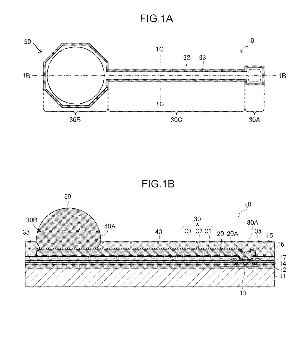
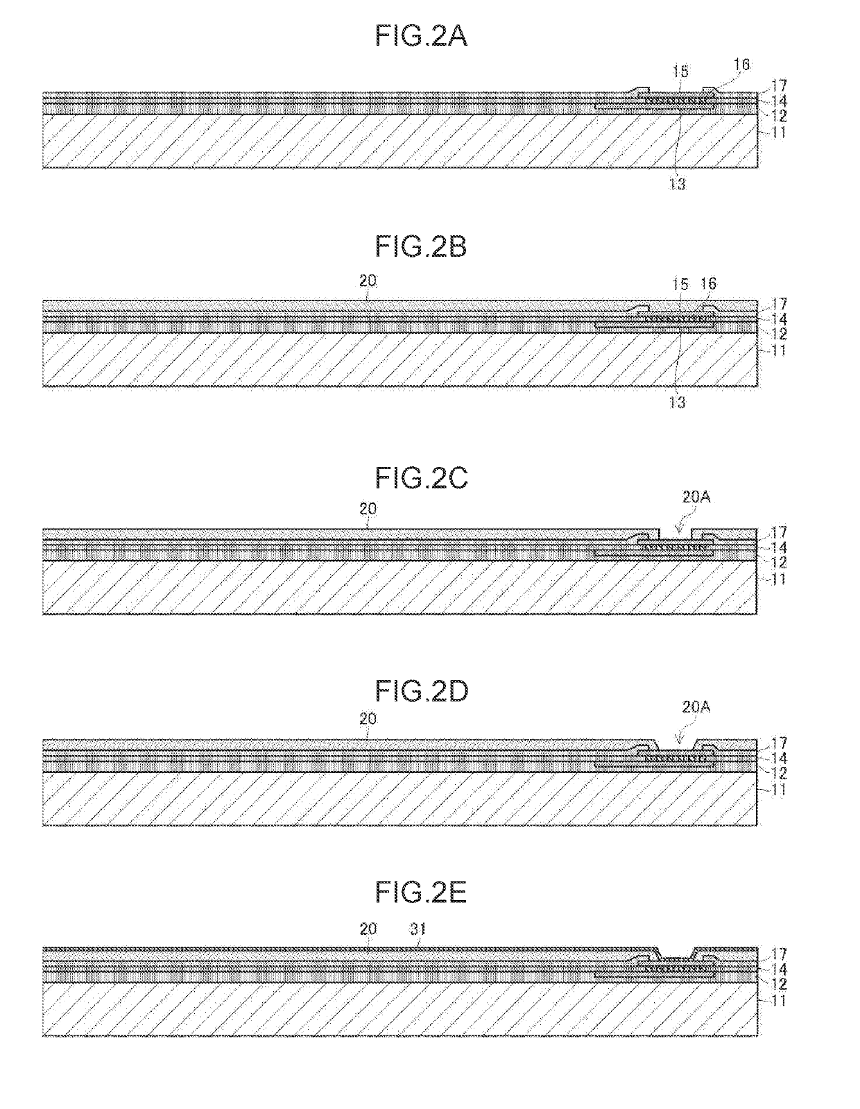
[0023]Hereinafter, exemplary embodiments of the disclosure will be described with reference to the drawings. In the drawings, substantially the same or equivalent components or portions are denoted by the same reference numerals.

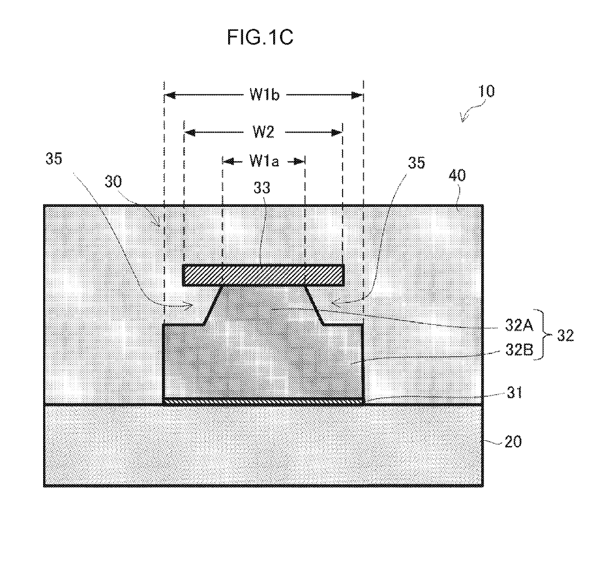
[0024]FIG. 1A is a plan view showing a configuration of an area for forming a redistribution 30 included in a semiconductor device 10 according to an exemplary embodiment of the disclosure. FIG. 1B is a cross-sectional view taken along line 1B-1B of FIG. 1A. FIG. 1C is a cross-sectional view taken along line 1C-1C of FIG. 1A. A lower insulating film 20, an upper insulating film 40, and an external connection terminal 50 shown in FIG. 1B are not shown in FIG. 1A.

[0025]The semiconductor device 10 includes a package which is similar to WL-CSP in shape. In other words, in the semiconductor device 10, a planar size of the package is substantially equal to a planar size of a semiconductor substrate 11. The semiconductor device 10 includes the lower insulating film...


PUM


Abstract

A semiconductor device includes: a wire including a first conductive member disposed at a semiconductor substrate and a second conductive member disposed at a surface of the first conductive member, the second conductive member having an ionization tendency less than the first conductive member, wherein the first conductive member includes a first surface disposed close to the second conductive member and having a width smaller than a width of a second surface of the first conductive member which is disposed close to the semiconductor substrate, and wherein the second conductive member has a width larger than the width of the first surface of the first conductive member and smaller than the width of the second surface of the first conductive member.

Description

CROSS-REFERENCE TO RELATED APPLICATION[0001]This application claims priority under 35 USC 119 from Japanese Patent Application No. 2017-209319, filed on Oct. 30, 2017, the disclosure of which is incorporated by reference herein.BACKGROUNDTechnical Field[0002]The present disclosure relates to a semiconductor device and a semiconductor device manufacturing method.Related Art[0003]Wafer level chip size package (WL-CSP) is packaging technology for semiconductor devices that implements redistribution, forming of electrode, resin sealing, and dicing, in wafer processes.[0004]For example, Japanese Patent Application Laid-Open (JP-A) No. 2015-138874 discloses a configuration of a semiconductor device provided with a redistribution, similarly to WL-CSP. In the semiconductor device disclosed in JP-A No. 2015-138874, the redistribution is disposed on an insulating film formed on a semiconductor substrate.[0005]A redistribution used in WL-CSP typically includes a Cu film. For the purpose of red...

Claims


Application Information

Patent Timeline
Patent Type & Authority Applications(United States)
IPC IPC(8): H01L23/31H01L21/02H01L21/311H01L21/78H01L21/66
CPCH01L23/3114H01L21/02164H01L21/0217H01L21/02274H01L21/31111H01L21/31144H01L21/78H01L22/32H01L22/34H01L2224/11H01L22/12H01L24/11H01L21/6836H01L2221/68327H01L2221/6834H01L2224/02166H01L24/03H01L24/05H01L2224/13111H01L24/13H01L2224/0401H01L2924/1304H01L2224/05548H01L2224/05552H01L2224/13014H01L2224/05166H01L2224/05147H01L2224/05644H01L2224/0347H01L2224/0361H01L2224/023H01L2924/01047H01L2924/00014H01L2924/00012H01L2924/0001
Inventor OGUMI, TAIICHI
Owner LAPIS SEMICON CO LTD
Why Eureka
Try Eureka