Wiring structure of semiconductor device

a technology of semiconductor devices and wiring structures, which is applied in the direction of semiconductor devices, semiconductor/solid-state device details, electrical devices, etc., can solve the problems of reducing the operating speed of semiconductor devices and misoperation of semiconductor devices

Inactive Publication Date: 2002-05-09
CONVERSANT INTPROP MANAGEMENT INC
View PDF5 Cites 0 Cited by
  • Summary
  • Abstract
  • Description
  • Claims
  • Application Information

AI Technical Summary

Benefits of technology

[0012] It is another objective of the present invention to provide a method for manufacturing the wiring structure of the semiconductor device by which it is possible to prevent the increase in the resistance of the wiring or the short in the wiring by preventing the wiring from being excessively etched when a planarizing method such as a CMP method is used.
[0020] According to the present invention, it is possible to prevent the excessive etching of the wiring and to pattern the wiring using a planarizing method such as the CMP method. Accordingly, it is possible to prevent the increase in the resistance of the wiring or the short in the wiring. Also, it is possible to use a multi-layer wiring structure, to secure a succeeding process margin, and stabilize a process.

Problems solved by technology

However, the conductive film may be over polished when it is polished by the CMP method and the first wiring 61 or the conductive stud 63 can be excessively etched by this over polishing phenomenon.
The increase of the resistance of the first wiring 61 can decrease the operating speed of the semiconductor device or cause misoperation of the semiconductor device.

Method used


Image

  • Wiring structure of semiconductor device
  • Wiring structure of semiconductor device
  • Wiring structure of semiconductor device

Examples


first embodiment

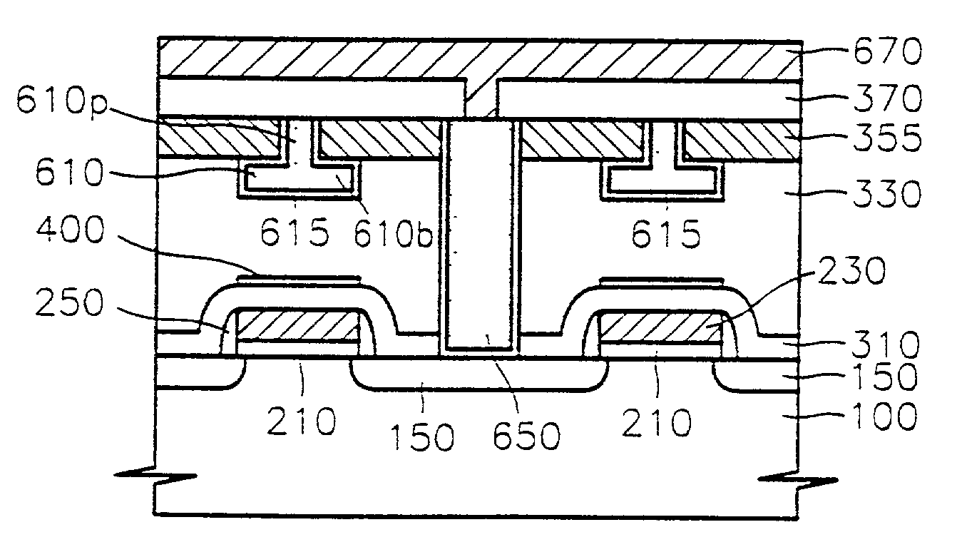
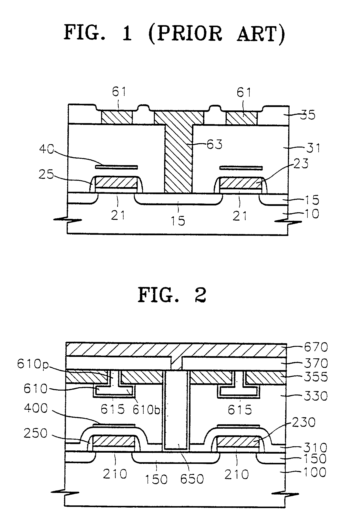
[0028] The wiring structure of an SRAM device according to the present invention will be described with reference to FIG. 2 in which a cross section of the SRAM device is shown. However, the present invention is not restricted to this embodiment. The present invention can be applied to various integrated circuits in which a multi-layer wiring structure is used.

[0029] To be specific, the wiring structure according to the first embodiment of the present invention has a first wiring 610 comprises a protrusion 610p formed on a body 610b to have a width less than that of the body 610b, and wherein an upper surface of protrusion 610p is planarized. The first wiring 610 can operate as a v.sub.ss line or a word line of the SRAM device. Therefore, though not shown in FIG. 2, the first wiring 610 is electrically connected to a gate electrode 230 or an active region 150 of a semiconductor substrate 100 by a conductive contact. Namely, the first wiring 610 is connected to the gate electrode 230...

second embodiment

[0059] A method of manufacturing the wiring structure of the SRAM device according to the present invention will be now described with reference to FIG. 10.

[0060] Referring to FIG. 10, the method of manufacturing the wiring structure of the SRAM device according to the second embodiment is different from the method of manufacturing the wiring structure of the SRAM device according to the first embodiment in that a process of forming a trench 355a is performed by a selective wet etching method. Accordingly, the trench 355a having a curved bottom is formed. This is due to the isotropic etching characteristic of the wet etching method. Other processes can proceed in the same way as the method of manufacturing the wiring structure of the SRAM device according to the first embodiment. As a result, the wiring structure shown in FIG. 9 can be formed.

[0061] It is possible to prevent an increase in resistance or generation of a short of the wiring caused by the over polishing or the excessiv...


PUM


Abstract

A wiring structure of a semiconductor device and a method for manufacturing the same are provided. The wiring structure according to the present invention includes a body formed of a first conductive material in a first insulating film on a semiconductor substrate and a protrusion formed of a second conductive material in a second insulating film formed on the first insulating film, connected to the upper surface of the body, formed to have a width less than that of the body, and having a planarized upper surface.

Description

[0001] This application is a divisional application of U.S. Pat. No. 09 / 359,243, filed on Jul. 22, 1999, which is herein incorporated by reference in its entirety.[0002] 1. Field of the Invention[0003] The present invention relates to a semiconductor device, and more particularly, to a wiring structure of a semiconductor device and a method for manufacturing the same.[0004] 2. Description of the Related Art[0005] As semiconductor devices become more highly integrated or the speed thereof increases, a multi-layer wiring structure is required. Accordingly, it is important to secure an alignment margin in a photolithography process for reducing the pitch of metal wiring or succeeding wiring. It is necessary to increase the flatness of an insulating film for insulating the metal wiring in order to reduce the pitch of the metal wiring or to secure the alignment margin.[0006] A process of planarizing the insulating film is necessary for increasing the flatness of the insulating film. For ...

Claims


Application Information

Patent Timeline
Patent Type & Authority Applications(United States)
IPC IPC(8): H01L21/28H01L21/768H01L21/8234H01L21/8244H01L21/3205H01L27/11
CPCH01L21/76804H01L21/7684H01L27/11H01L21/823425H01L21/823475H01L21/76877H10B10/00H01L21/28
Inventor MOON, JAE-HWANKIM, GYU-CHUL
Owner CONVERSANT INTPROP MANAGEMENT INC
Why Eureka
Try Eureka