Dry etching method

a technology of dry etching and etching plate, which is applied in the direction of basic electric elements, electrical equipment, chemistry apparatus and processes, etc., can solve the problems of anomalous etching shape, etching not lasting, and anomalous etching shap

Active Publication Date: 2022-02-15
CENT GLASS CO LTD
View PDF12 Cites 0 Cited by
  • Summary
  • Abstract
  • Description
  • Claims
  • Application Information

AI Technical Summary

Benefits of technology

[0016]On the other hand, it is described in Patent Document 2 that the use of the etching gas containing HFO-1234ze(E), the unsaturated perfluorocarbon CxFy (where x is an integer of 2 to 5; y is 2, 4, 6, 8 or 10; and x and y satisfy y≤2x) and the oxidizing gas makes it possible to effectively control the etching rates of the SiN and SiOx layers and suppress the occurrence of anomaly in etching shape.
[0017]By the way, it is common practice in the production of ordinary semiconductor devices to lengthen etching time by about 1.1 to 2 times and thereby perform etching treatment more than necessary in order to prevent poor contact (electrical conduction) caused due to a residue of the etched layer at the bottom part of the etched hole. On the other hand, an etch stop layer is formed in advance at the hole bottom part in order to prevent excessive etching. The same goes for the production of devices with so-called 3D NAND structures. In other words, it is necessary, even in the above-mentioned laminated film etching method where the etching process takes place with a high aspect ratio over a depth of several μm, to stop excessive etching by forming an etch stop layer of about several nm to several tens nm at the hole bottom part, that is, the bottom part of the through hole.
[0019]The present inventors have tried the method disclosed in Patent Document 2 and resultantly found that: the method disclosed in Patent Document 2 enables high-aspect-ratio etching without causing anomaly in etching shape, but causes excessive deposition of a fluorocarbon film on the etch stop layer; and the deposited fluorocarbon film remains as an etching residue which can result in poor contact at the hole bottom part.
[0021]In view of these circumstances, there has been a demand for an etching method capable of etching with a high aspect ratio of 20 or higher without causing anomaly in etching shape and without causing excessive deposition on an etch stop layer.
[0023]As a result of extensive researches made to achieve the above object, the present inventors have found that, in a process of forming a through hole vertically in an etching target film in which a plurality of SiN and SiOx layers are alternately laminated together on a substrate, the adoption of plasma etching using a dry etching agent which contains at least C3F6 and a hydrogen-containing saturated fluorocarbon of 1 to 4 carbons at a predetermined ratio makes it possible to freely control a value of dividing an etching rate of SiN by an etching rate of SiOx (SiN / SiOx etching rate ratio) within the range of 0.90 to 1.5 and possible to suppress excessive deposition on an etch stop layer while ensuring selectivity to the etch stop layer. The present disclosure is based on this finding.

Problems solved by technology

However, the method disclosed in Patent Document 1 fails to show sufficient etching selectivity to the mask and thus has a problem that, when the laminated film is large in thickness, the mask does not last until the completion of the etching operation.
The method disclosed in Patent Document 1 also has a problem of anomaly in etching shape, such as bowing, being caused due to the insufficient formation of a side wall protecting film during the etching operation.
Especially when the etching rate of the SiN layer is excessively high as compared to the etching rate of the SiOx layer, isotropic etching of the SiN layers proceeds in addition to anisotropic etching and becomes a cause of anomaly in etching shape.
Further, the method using the plasma generated from hexafluoropropene and oxygen gas as disclosed in Patent Document 4 is not suitable for formation of a through hole in a laminated film of SiN and SiO2 layers because the plasma used exhibits a higher etching rate of silicon oxide than that of silicon nitride as shown in Comparative Example 1 of the present application.

Method used


Image

  • Dry etching method
  • Dry etching method
  • Dry etching method

Examples


example 1

[0061](Etching Operation)

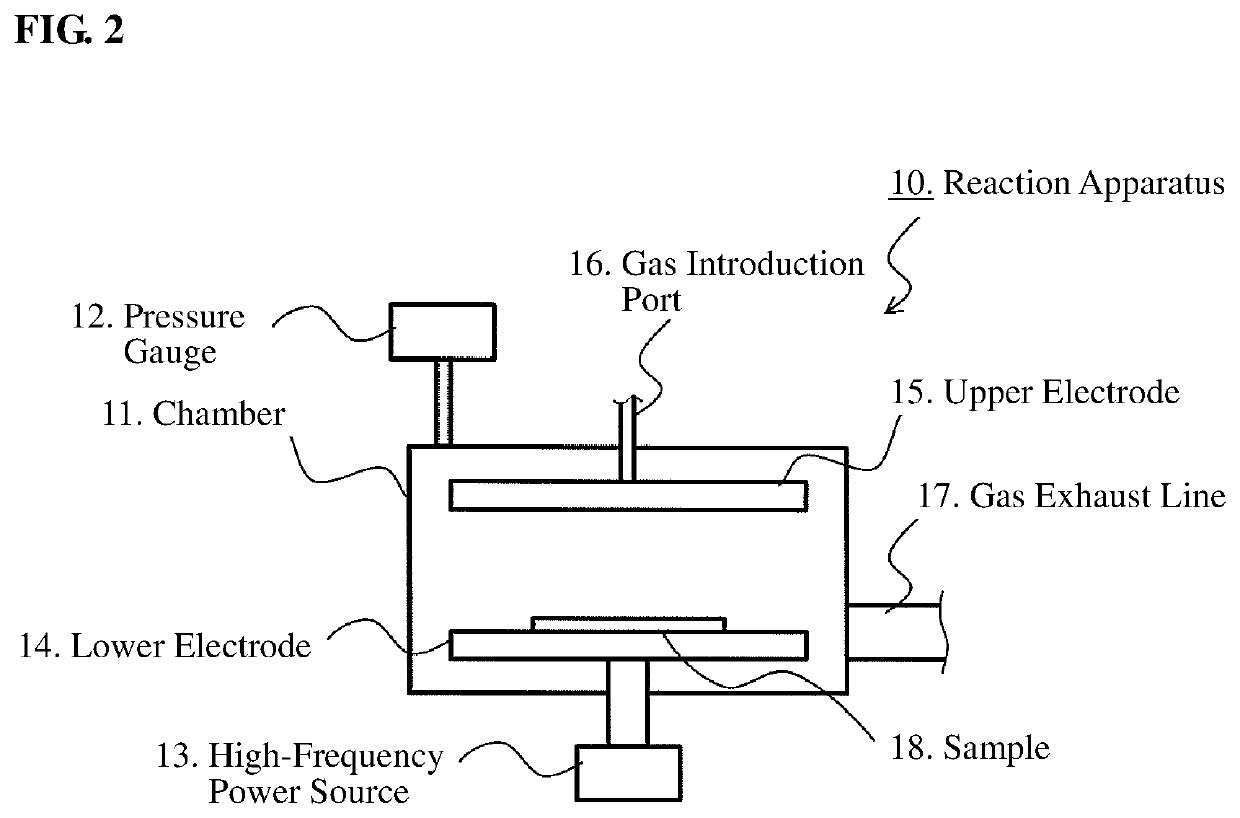
[0062]FIG. 2 is a schematic view of a reaction apparatus 10 used in Examples and Comparative Examples. In a chamber 11, a lower electrode 14, an upper electrode 15 and a pressure gauge 12 were arranged. Herein, the lower electrode 14 had the function of holding a sample 18 and thus also served as a stage. A gas introduction port 16 was connected to an upper part of the chamber 11. The chamber 11 was configured to control its inside pressure and to plasmatize a dry etching agent by means of a high-frequency power source (13.56 MHz) 13. Accordingly, the sample 18 was etched by bringing the plasmatized dry etching agent into contact with the sample 18 on the lower electrode 14. With the application of a high-frequency power from the high-frequency power source 13 in a state that the dry etching agent was introduced into the chamber, there was developed a direct-current voltage, called a self-bias voltage, between the upper electrode 15 and the lower electrode 1...


PUM

PropertyMeasurementUnit
self-bias voltageaaaaaaaaaa
bias voltageaaaaaaaaaa
aspect ratioaaaaaaaaaa

Abstract

A dry etching method according to the present disclosure is for forming a through hole in a laminated film of silicon oxide layers and silicon nitride layers on a substrate in a direction vertical to the laminated film by plasmatizing a dry etching agent to generate a plasma and etching the laminated film by the plasma through a mask having a predetermined opening pattern under a negative direct-current self-bias voltage whose absolute value is 500 V or greater, wherein the dry etching agent contains at least C3F6, a hydrogen-containing saturated fluorocarbon represented by CxHyFz and an oxidizing gas, and wherein the volume of the hydrogen-containing saturated fluorocarbon contained in the dry etching agent is in a range of 0.1 to 10 times the volume of C3F6 contained in the dry etching agent.

Description

FIELD OF THE INVENTION[0001]The present disclosure relates to a dry etching method using a dry etching agent that contains a fluorine-containing unsaturated hydrocarbon.BACKGROUND ART[0002]In the manufacturing of semiconductor devices, fine processing is nowadays approaching physical limits. In order to compensate for such limits, there has been developed a technique to integrate semiconductor devices by stacking structural elements in height directions. This integration tendency is particularly notable in NAND flash memories. The research and development of three-dimensional NAND flash memories are being actively pursued.[0003]For example, a three-dimensional NAND flash memory is known including: a substrate; a laminated film having a plurality of polycrystalline silicon (referred to as poly-Si or p-Si) layers and silicon oxide (referred to as SiOx) layers alternately laminated on the substrate; and an electrode element embedded vertically in the laminated film. In the case of prod...

Claims


Application Information

Patent Timeline
Patent Type & Authority Patents(United States)
IPC IPC(8): H01L21/311H01L21/02H01L21/3065
CPCH01L21/31116H01L21/0212H01L21/3065H01L21/31144H10B41/27H10B43/20H01L21/02164H01L21/0217C09K13/00H10B43/27
Inventor OOMORI, HIROYUKISUZUKI, SHOI
Owner CENT GLASS CO LTD
Why Eureka
Try Eureka