Integrated circuit memory devices having impurity-doped dielectric regions therein and methods of forming same

a technology of integrated circuit memory and impurity-doped dielectric region, which is applied in the direction of semiconductor devices, semiconductor/solid-state device details, electrical apparatus, etc., can solve the problem of increasing the defect rate of three-dimensional semiconductor devices, and achieve the effect of improving the integration density and improving the distribution properties

Active Publication Date: 2019-05-23
SAMSUNG ELECTRONICS CO LTD
View PDF0 Cites 5 Cited by
  • Summary
  • Abstract
  • Description
  • Claims
  • Application Information

AI Technical Summary

Benefits of technology

[0004]An aspect of the present inventive concept may provide a semiconductor device that supports increases in integration density, and may improve distribution properties.

Problems solved by technology

As the constituent elements of the three-dimensional semiconductor devices have a more compact size in order to increase the degree of integration of three-dimensional semiconductor devices, the defect rate of three-dimensional semiconductor devices has increased.

Method used


Image

  • Integrated circuit memory devices having impurity-doped dielectric regions therein and methods of forming same
  • Integrated circuit memory devices having impurity-doped dielectric regions therein and methods of forming same
  • Integrated circuit memory devices having impurity-doped dielectric regions therein and methods of forming same

Examples


Embodiment Construction

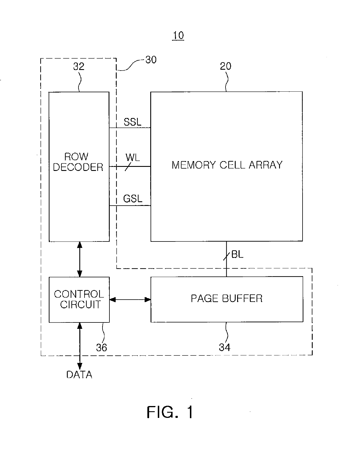
[0024]An example of a semiconductor device, according to an example embodiment of the present inventive concept, will be described with reference toFIG. 1, which is a schematic block diagram of the semiconductor device. Referring to FIG. 1, a semiconductor device 10, according to an example embodiment, may include a memory cell array region 20 and a control logic region 30. The memory cell array region 20 may include a plurality of memory blocks, and each of the memory blocks may include a plurality of memory cells. The control logic region 30 may include a row decoder 32, a page buffer 34, and a control circuit 36.

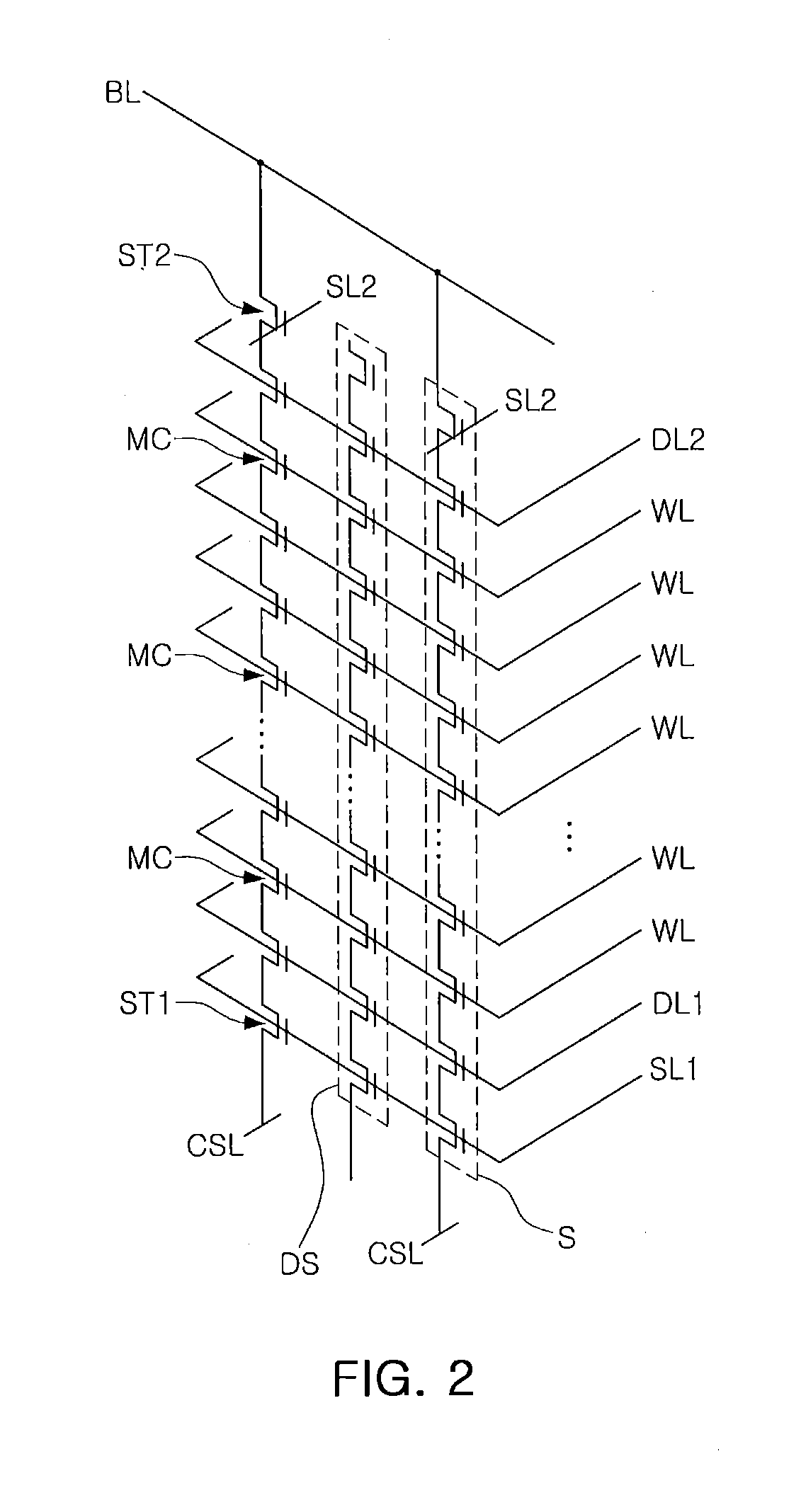
[0025]The memory cells of the memory cell array region 20 may be connected to the row decoder 32 via a string select line SSL, a plurality of word lines WLs, and a ground select line GSL, and may be connected to the page buffer 34 via bit lines BLs. In example embodiments, a plurality of memory cells arranged in an identical row may be connected to an identical word line ...


PUM


Abstract

An integrated circuit memory device includes a vertical stack structure containing an interlayer insulating layer and a gate electrode, on a substrate. A blocking dielectric region is provided on a sidewall of an opening in the stack structure. A lateral impurity region is provided, which extends between the blocking dielectric region and the interlayer insulating layer and between the blocking dielectric region and the gate electrode. A lower impurity region is also provided, which extends between the blocking dielectric region and the substrate.

Description

REFERENCE TO PRIORITY APPLICATION[0001]This application claims priority to Korean Patent Application No. 10-2017-0155585, filed Nov. 21, 2017, the disclosure of which is hereby incorporated herein by reference in its entirety.BACKGROUND1. Field[0002]The present inventive concept relates to semiconductor devices and more particularly, to semiconductor devices having impurity regions therein.2. Description of Related Art[0003]The degree of integration of semiconductor devices, such as flash memories, is an important factor that may determine the price of semiconductor products. A three-dimensional semiconductor device, including memory cells arranged three-dimensionally, has been proposed, together with a large semiconductor wafer, in order to increase the degrees of integration of such semiconductor devices. As the constituent elements of the three-dimensional semiconductor devices have a more compact size in order to increase the degree of integration of three-dimensional semiconduc...

Claims


Application Information

Patent Timeline
Patent Type & Authority Applications(United States)
IPC IPC(8): H01L27/11582H01L29/06H01L29/10H01L29/51H01L23/528H01L23/522H01L21/311H01L21/3115H01L21/28H01L21/02
CPCH01L27/11582H01L29/0649H01L29/1037H01L29/513H01L23/528H01L23/5226H01L21/31111H01L21/3115H01L21/28282H01L21/0223H01L27/11565H01L29/518H10B43/35H10B43/27H01L29/788H01L21/22H10B41/35H10B41/41H10B41/20H01L29/40117H10B43/10
Inventor JANG, WOO JINNOH, YOUNG JINYANG, JUN KYUKIM, BIOAN, KYONG WON
Owner SAMSUNG ELECTRONICS CO LTD
Why Eureka
Try Eureka