Semiconductor memory device and method of fabricating the same

a memory device and semiconductor technology, applied in semiconductor devices, semiconductor/solid-state device details, electrical apparatus, etc., can solve the problems of difficult integration of high-end semiconductor devices, and achieve the effect of increasing the process margin of landing pads and enhancing reliability

Active Publication Date: 2019-05-30
SAMSUNG ELECTRONICS CO LTD
View PDF2 Cites 22 Cited by
  • Summary
  • Abstract
  • Description
  • Claims
  • Application Information

AI Technical Summary

Benefits of technology

[0004]Exemplary embodiments of the present inventive concept provide a semiconductor memory device having enhanced reliability, and also provide a method of fabricating the semiconductor memory device in which a process margin for landing pads is increased.

Problems solved by technology

However, since new exposure techniques and / or expensive exposure systems may be required for printing these tine patterns, to highly integrate the semiconductor devices may not be easy.

Method used


Image

  • Semiconductor memory device and method of fabricating the same
  • Semiconductor memory device and method of fabricating the same
  • Semiconductor memory device and method of fabricating the same

Examples


Embodiment Construction

[0019]Hereinafter, some exemplary embodiments of the present inventive concept will be described in detail in conjunction with the accompanying drawings to aid in clearly explaining the present inventive concept.

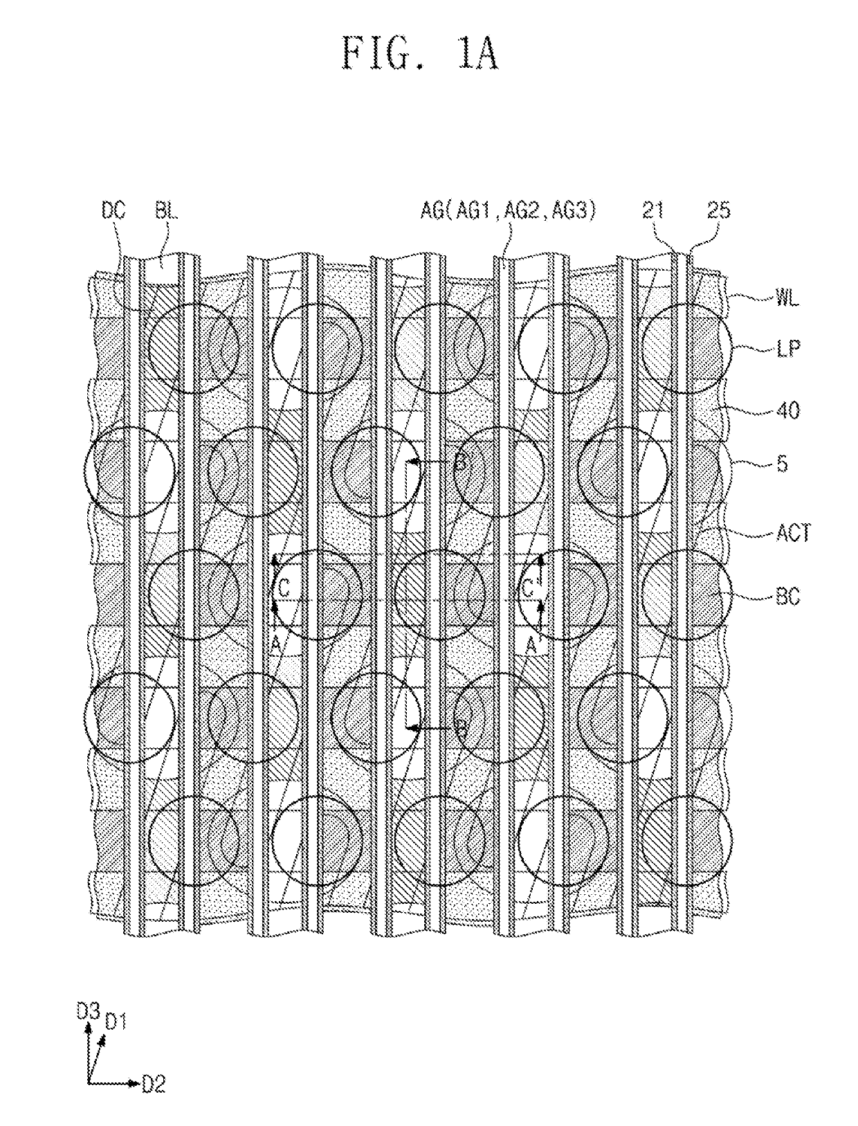
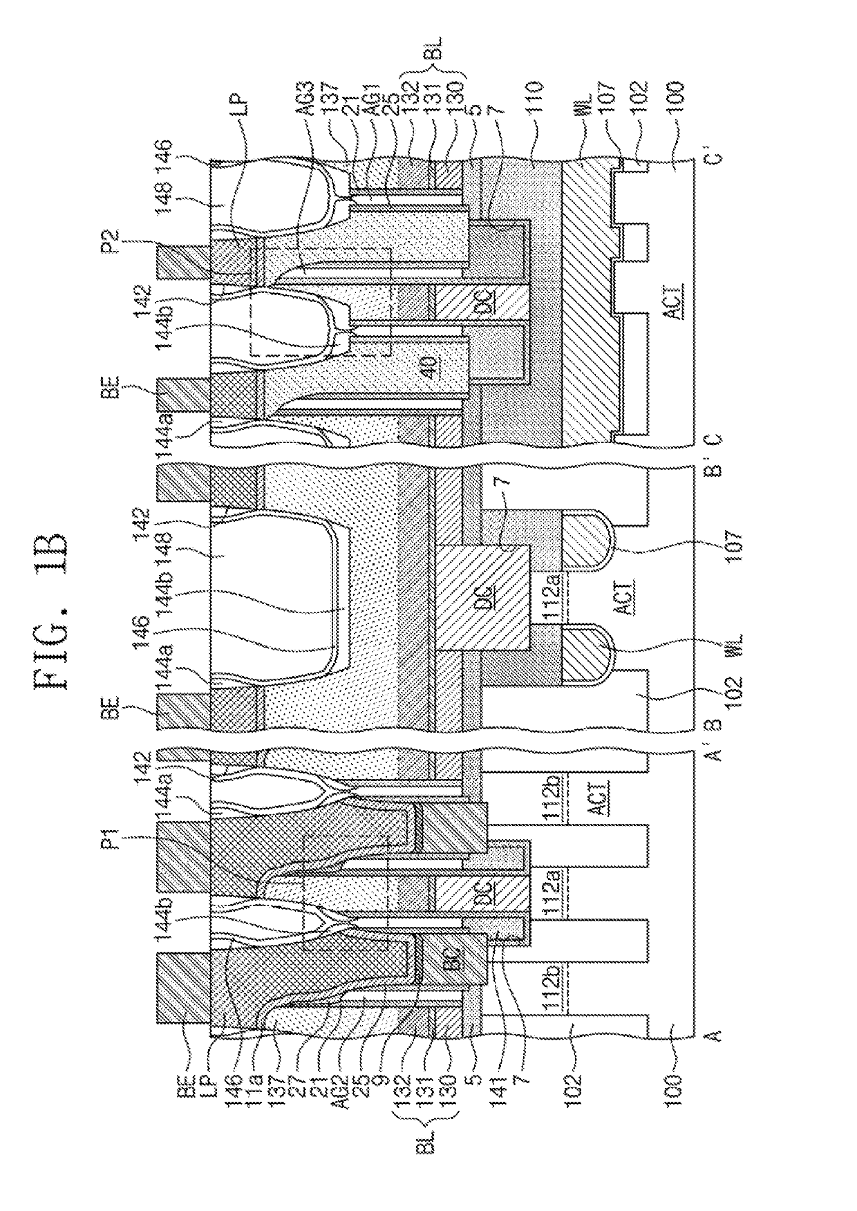
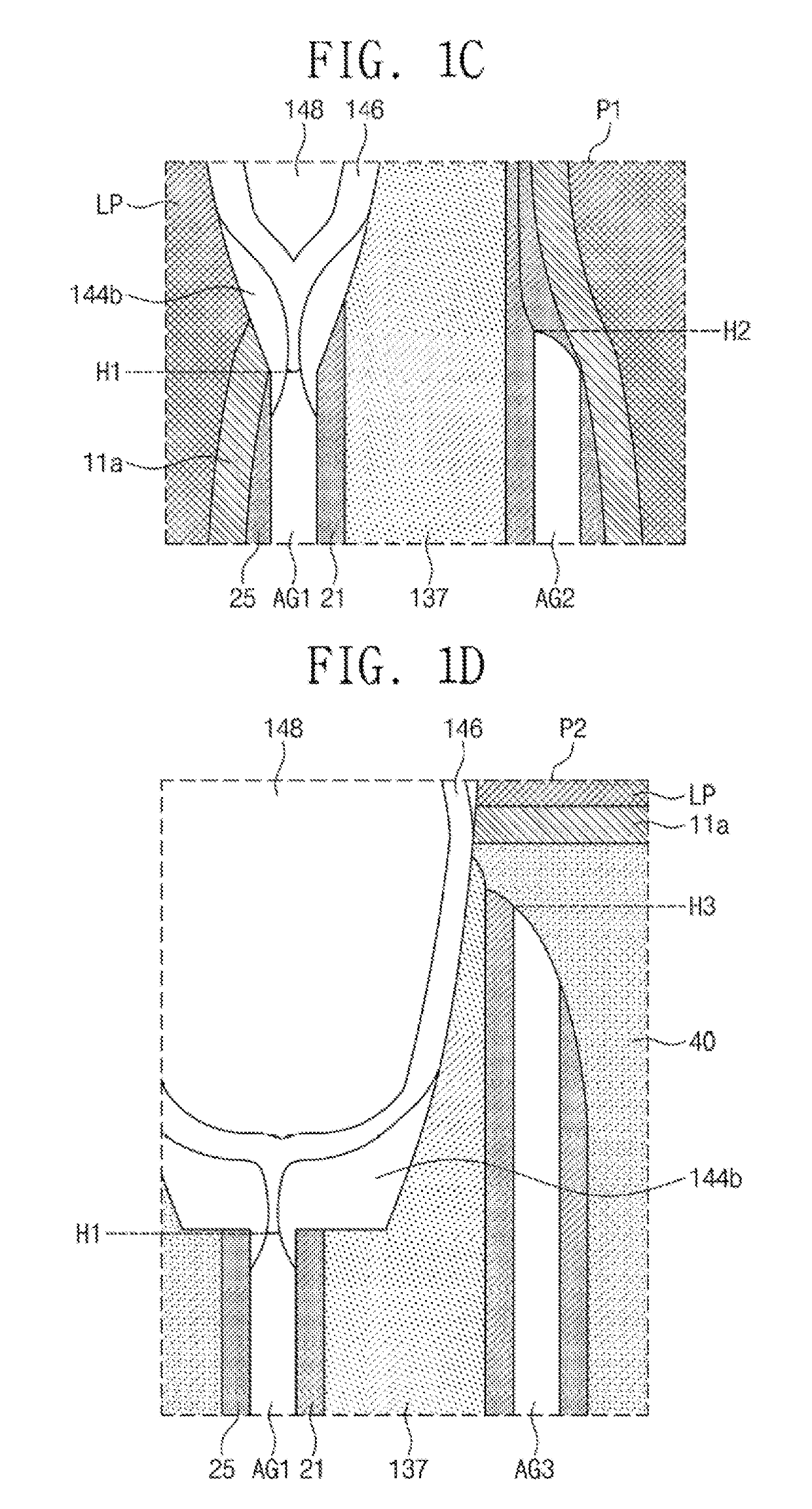
[0020]FIG. 1A is a plan view showing a semiconductor memory device according to an exemplary embodiment of the present inventive concept. FIG. 1B is a partial cross-sectional view of FIG. 1A, FIG. IC is an enlarged view showing section P1 of FIG. 1B. FIG. 1D is an enlarged view showing section P2 of FIG. 1B. FIG. 1B shows cross-sections taken along lines A-A′, B-B′, and C-C′ of FIG. 1A.

[0021]Referring to FIGS. IA to ID, a semiconductor substrate 100 (referred to hereinafter as a substrate) may be provided therein with device isolation patterns 102 defining active sections ACT. Each of the active sections ACT may have an isolated shape, and may have a bar shape elongated along a first direction DI in a plan view. When viewed in plan, the active sections ACT may correspond to ...


PUM


Abstract

Provided are a semiconductor memory device and a method of fabricating the same. The semiconductor memory device may include: a first impurity doped region and a second impurity doped region spaced apart from each other in a semiconductor substrate, a bit line electrically connected to the first impurity doped region and crossing over the semiconductor substrate, a storage node contact electrically connected to the second impurity doped region, a first spacer and a second spacer disposed between the bit line and the storage node contact, and an air gap region disposed between the first spacer and the second spacer. The first spacer may cover a sidewall of the bit line, and the second spacer may be adjacent to the storage node contact. A top end of the first spacer may have a height higher than a height of a top end of the second spacer.

Description

CROSS-REFERENCE TO RELATED APPLICATIONS[0001]This U.S. nonprovisional application claims priority under 35 U.S.C. § 119 to Korean Patent Application No. 10-2017-0161929, filed on Nov. 29, 2017, in the Korean Intellectual Property Office, the disclosure of which is herein incorporated by reference in its entirety.TECHNICAL FIELD[0002]The present inventive concept relates to a semiconductor memory device and a method of fabricating the same.DISCUSSION OF RELATED ART[0003]Semiconductor devices have been widely used in electronic industry because of their small size, multi-functionality, and / or low fabrication cost. As the semiconductor devices become increasingly integrated with the advancement of the electronic industry, line widths of patterns of the semiconductor devices are being reduced for high integration thereof. However, since new exposure techniques and / or expensive exposure systems may be required for printing these tine patterns, to highly integrate the semiconductor device...

Claims


Application Information

Patent Timeline
Patent Type & Authority Applications(United States)
IPC IPC(8): H01L27/108H01L23/532H01L29/06
CPCH01L27/10805H01L27/10885H01L27/10888H01L23/5329H01L29/0649H01L27/22H01L27/24H10B63/30H10B61/22H10B12/315H10B12/485H10B12/482H01L27/105H01L21/7682H01L21/76816H01L21/76831H10B12/30H10B61/00H10B63/00H10N59/00
Inventor SONG, JUNGWOOKIM, KWANGMINLEE, JUN HOKANG, HYUCKJINKIM, YONG KWANHAN, SANGYEONPARK, SEGUEN
Owner SAMSUNG ELECTRONICS CO LTD
Why Eureka
Try Eureka