Structure with micro device

a micro-device and structure technology, applied in the field of structure with micro-devices, to achieve the effect of improving transportation and transfer yield

Active Publication Date: 2019-06-20
PLAYNITRIDE
View PDF2 Cites 6 Cited by
  • Summary
  • Abstract
  • Description
  • Claims
  • Application Information

AI Technical Summary

Benefits of technology

[0004]The invention provides a structure with micro device capable of effectively improving a transportation and transfer yield of micro devices.

Problems solved by technology

However, positions where the holding structures are disposed on the micro LEDs may influence a transportation and transfer yield of the micro LEDs.

Method used


Image

  • Structure with micro device
  • Structure with micro device
  • Structure with micro device

Examples


Embodiment Construction

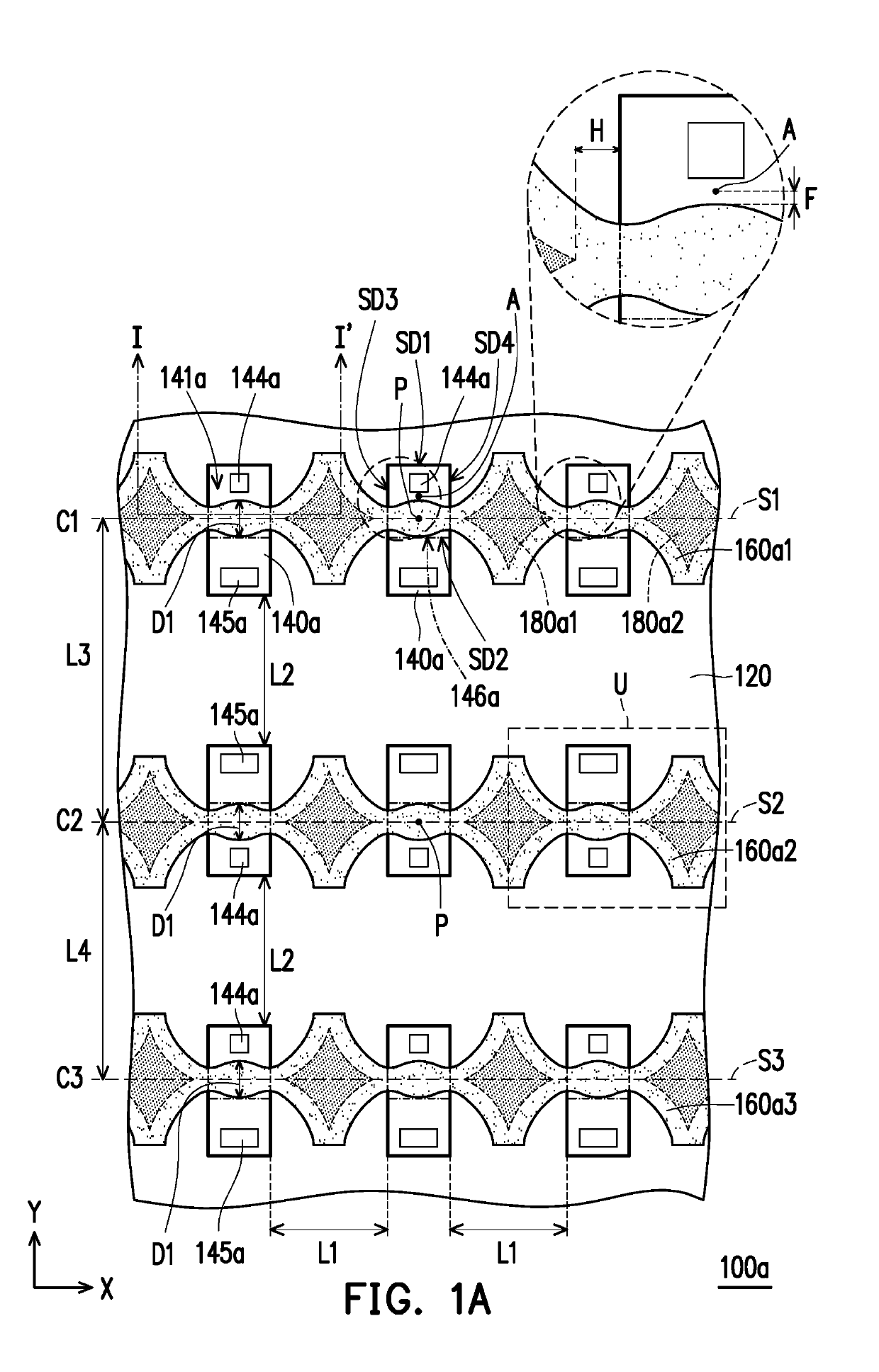
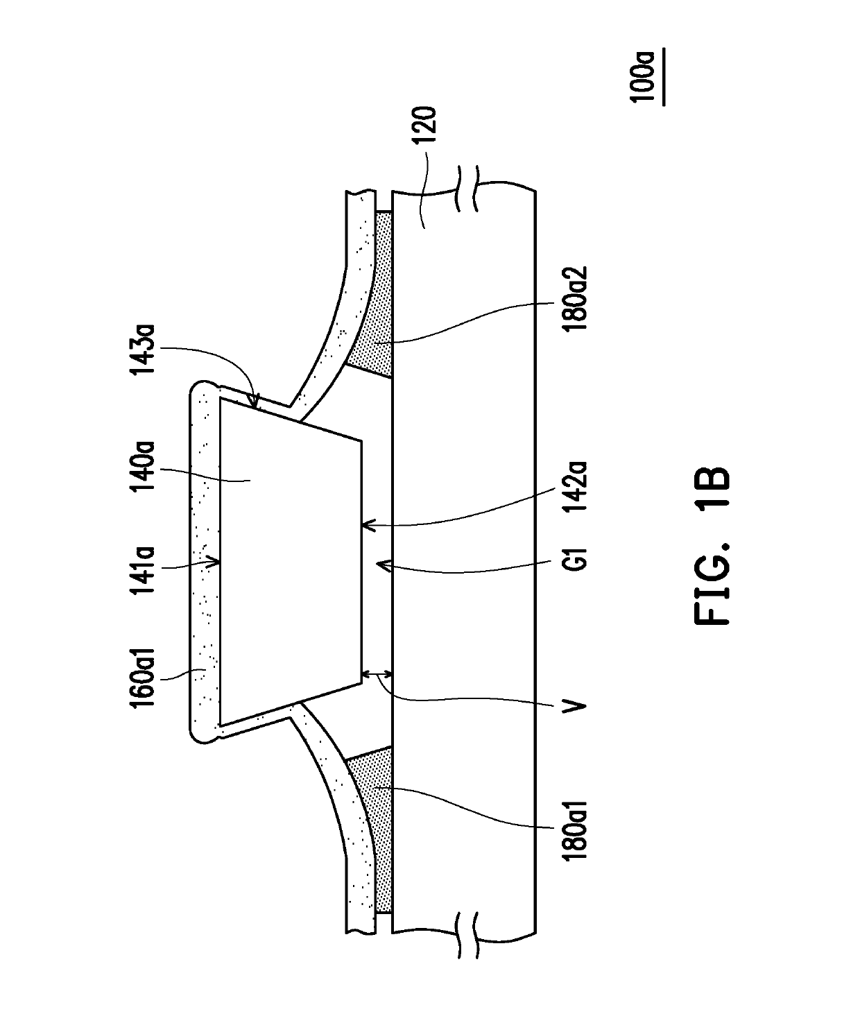
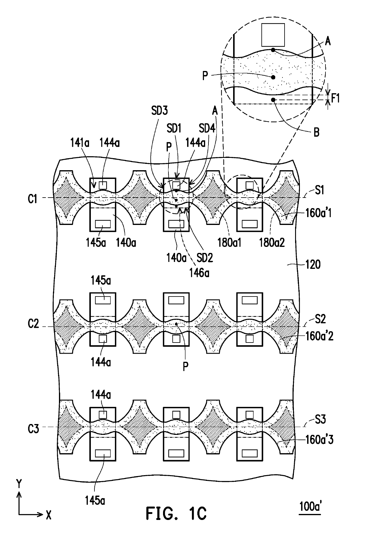
[0035]The embodiments of the invention describe a structure of micro devices (e.g., micro light emitting diodes (LEDs) and microchips) which are ready to be picked up and transferred to a circuit substrate. For example, a receiving substrate may be a display substrate, a light-emitting substrate, a substrate having functional devices, such as transistors or integrated circuits (ICs) or a substrate having metal redistribution lines, which is not limited in the invention. Even though some of the embodiments of the invention are specific to describe micro LEDs including p-n diodes, it should be understood that the embodiments of the invention are not limited thereto, and some of the embodiments may also be applied to other micro semiconductor devices. Those devices may be designed according to such manner to control execution of a predetermined electron function (e.g., diode, transistor, integrated circuit) or photon function (e.g., LED, laser). FIG. 1A is a schematic top view of a str...


PUM


Abstract

A structure with micro device includes a substrate, a plurality of micro devices, and a plurality of holding structures. The micro devices are disposed on the substrate and arranged in multiple rows. Each of the micro devices has a top surface. The holding structures are respectively disposed on the top surface of each of the micro devices and extend to the substrate. Distances between the holding structure on the micro devices on any one of the rows and the holding structures on the micro devices on two adjacent rows are different.

Description

CROSS-REFERENCE TO RELATED APPLICATION[0001]This application claims the priority benefits of U.S. provisional application Ser. No. 62 / 607,325, filed on Dec. 19, 2017 and Taiwan application serial no. 107119258, filed on June 5, 2018. The entirety of each of the above-mentioned patent applications is hereby incorporated by reference herein and made a part of this specification.BACKGROUNDField of the Invention[0002]The invention relates to a semiconductor structure, and more particularly, to a structure with micro device.Description of Related Art[0003]At present, transferring micro light-emitting diodes (LEDs) from a carrier to a receiving substrate is mainly done via an electrostatic force or a magnetic force. In general, micro LEDs are held by holding structures, so that it is easier for the micro LEDs to be picked up from the substrate, transported and transferred to be placed on the receiving substrate, and the micro LEDs are secured by the holding structures to prevent the quali...

Claims


Application Information

Patent Timeline
Patent Type & Authority Applications(United States)
IPC IPC(8): H01L25/13H01L33/48
CPCH01L25/13H01L33/483H01L25/0753H01L33/0095H01L2924/12041H01L2224/95001H01L2224/0603H01L2224/05554H01L2224/05553H01L2924/00014H01L24/95H01L24/05H01L24/06H01L2221/68368H01L21/6835H01L2221/68313H01L2924/00012H01L2224/05599H01L24/00
Inventor WU, CHIH-LINGSU, YI-MINLO, YU-YUN
Owner PLAYNITRIDE
Why Eureka
Try Eureka