Reducing latency of memory read operations returning data on a read data path across multiple clock boundaries, to a host implementing a high speed serial interface

a memory read and serial interface technology, applied in the field of memory system calibration, can solve the problems of affecting the performance the potential to significantly affect the timing margins of the computer system, so as to and minimize the latency of the read data path

Active Publication Date: 2019-07-11
IBM CORP
View PDF0 Cites 25 Cited by
  • Summary
  • Abstract
  • Description
  • Claims
  • Application Information

AI Technical Summary

Benefits of technology

[0003]In one embodiment, a method is directed to determining, by a computer system, a latest arriving data strobe at a first data buffer in a read data path between at least one memory chip and a host on a high speed interface. The method is directed to aligning, by the computer system, a chip clock distributed to a second data buffer in the read data path with the latest arriving data strobe, wherein data crosses a first clock boundary from the first data buffer to the second data buffer, to minimize a latency in the read data path across the first clock boundary. The method is directed to aligning, by the computer system, the chip clock with a high speed clock for controlling an unload pointer to unload data from the second data buffer to a serializer in the read data path, wherein data crosses a second clock boundary from the second data buffer to the serializer, to minimize a latency in the read data path across a second clock boundary.
[0004]In another embodiment, a computer system comprises one or more processors, one or more computer-readable memories, one or more computer-readable storage devices, and program instructions, stored on at least one of the one or more storage devices for execution by at least one of the one or more processors via at least one of the one or more memories. The stored program instructions comprise program instructions to determine a latest arriving data strobe at a first data buffer in a read data path between at least one memory chip and a host on a high speed interface. The stored program instructions comprise program instructions to align a chip clock distributed to a second data buffer in the read data path with the latest arriving data strobe, wherein data crosses a first clock boundary from the first data buffer to the second data buffer, to minimize a latency in the read data path across the first clock boundary. The stored program instructions comprise program instructions to align the chip clock with a high speed clock for controlling an unload pointer to unload data from the second data buffer to a serializer in the read data path, wherein data crosses a second clock boundary from the second data buffer to the serializer, to minimize a latency in the read data path across a second clock boundary.
[0005]In another embodiment, a computer program product comprises one or more computer-readable storage devices and program instructions, stored on at least one of the one or more storage devices. The stored program instructions comprise program instructions to determine a latest arriving data strobe at a first data buffer in a read data path between at least one memory chip and a host on a high speed interface. The stored program instructions comprise program instructions to align a chip clock distributed to a second data buffer in the read data path with the latest arriving data strobe, wherein data crosses a first clock boundary from the first data buffer to the second data buffer, to minimize a latency in the read data path across the first clock boundary. The stored program instructions comprise program instructions to align the chip clock with a high speed clock for controlling an unload pointer to unload data from the second data buffer to a serializer in the read data path, wherein data crosses a second clock boundary from the second data buffer to the serializer, to minimize a latency in the read data path across a second clock boundary.

Problems solved by technology

Timing variations, frequency, temperature, aging and other conditions impact data transfer rates to and from memory or other storage, which impacts computer system performance.
In addition, in a computer system where a host implements an serializer / deserializer (SerDes) based, high speed serial (HSS) interface for interfacing between a memory device operating under a first memory protocol and a host that is agnostic to the first memory protocol, for asynchronous read operations, timing variations between clock and data signals along a read data return path have the potential to significantly impact timing margins within the computer system.

Method used


Image

  • Reducing latency of memory read operations returning data on a read data path across multiple clock boundaries, to a host implementing a high speed serial interface
  • Reducing latency of memory read operations returning data on a read data path across multiple clock boundaries, to a host implementing a high speed serial interface
  • Reducing latency of memory read operations returning data on a read data path across multiple clock boundaries, to a host implementing a high speed serial interface

Examples


Embodiment Construction

[0016]In the following description, for the purposes of explanation, numerous specific details are set forth to provide a thorough understanding of the present invention. It will be apparent, however, to one skilled in the art that the present invention may be practiced without these specific details. In other instances, well-known structures and devices are shown in block diagram form to avoid unnecessarily obscuring the present invention.

[0017]In addition, in the following description, for purposes of explanation, numerous systems are described. It is important to note, and it will be apparent to one skilled in the art, that the present invention may execute in a variety of systems, including a variety of computer systems and electronic devices operating any number of different types of operating systems.

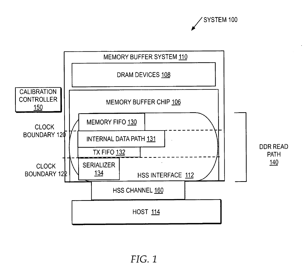
[0018]FIG. 1 illustrates a block diagram of a system including multiple clock boundaries between at least one memory buffer system and a host, across an HSS interface.

[0019]In one...


PUM


Abstract

A calibration controller determines a latest arriving data strobe at a first data buffer in a read data path between at least one memory chip and a host on a high speed interface. The calibration controller aligns a chip clock distributed to a second data buffer in the read data path with the latest arriving data strobe, wherein data crosses a first clock boundary from the first data buffer to the second data buffer, to minimize a latency in the read data path across the first clock boundary. The calibration controller aligns the chip clock with a high speed clock for controlling an unload pointer to unload data from the second data buffer to a serializer in the read data path, wherein data crosses a second clock boundary from the second data buffer to the serializer, to minimize a latency in the read data path across a second clock boundary.

Description

BACKGROUND1. Technical Field[0001]This invention relates in general to a memory system calibration and more particularly to reducing latency of memory read operations returning data on a read data path across multiple clock boundaries, to a host implementing a high speed serial interface.2. Description of the Related Art[0002]Computing systems generally include one or more circuits with one or more memory or storage devices connected to one or more processors via one or more controllers. Timing variations, frequency, temperature, aging and other conditions impact data transfer rates to and from memory or other storage, which impacts computer system performance. In addition, in a computer system where a host implements an serializer / deserializer (SerDes) based, high speed serial (HSS) interface for interfacing between a memory device operating under a first memory protocol and a host that is agnostic to the first memory protocol, for asynchronous read operations, timing variations be...

Claims


Application Information

Patent Timeline
Patent Type & Authority Applications(United States)
IPC IPC(8): G06F1/12G06F1/10G06F1/08G06F13/16H03L7/085G11C7/22
CPCG06F1/12G06F1/10G06F1/08G06F13/1673G06F13/1689H03L7/085G11C7/222G11C2207/2254G11C2207/2272
Inventor CARLOUGH, STEVEN R.EICKHOFF, SUSAN M.SPEAR, MICHAEL B.VAN HUBEN, GARY A.WYATT, STEPHEN D.
Owner IBM CORP
Why Eureka
Try Eureka