Displaying apparatus having light emitting device, method of manufacturing the same and method of transferring light emitting device

a technology display panels, which is applied in the manufacture of electrical apparatus, semiconductor/solid-state devices, and semiconductor devices. it can solve the problems of difficult mounting of light emitting diodes on display panels, difficult handling of light emitting diodes of a small size, etc., and achieves the effect of convenient mounting

Active Publication Date: 2019-07-25
SEOUL SEMICONDUCTOR
View PDF11 Cites 39 Cited by
  • Summary
  • Abstract
  • Description
  • Claims
  • Application Information

AI Technical Summary

Benefits of technology

[0008]Exemplary embodiments of the inventive concepts provide a method of manufacturing a displaying apparatus by which a plurality of light emitting devices formed on a growth substrate can be easily mounted on a display panel substrate and a displaying apparatus manufactured through the method.

Problems solved by technology

However, the micro LED whose size is less than 200 microns, further less than 100 microns is very small, and various problems occur because of these small sizes.
In particular, it is difficult to handle light emitting diodes of a small size and it is not easy to mount a light emitting diode on a display panel.

Method used


Image

  • Displaying apparatus having light emitting device, method of manufacturing the same and method of transferring light emitting device
  • Displaying apparatus having light emitting device, method of manufacturing the same and method of transferring light emitting device
  • Displaying apparatus having light emitting device, method of manufacturing the same and method of transferring light emitting device

Examples


Embodiment Construction

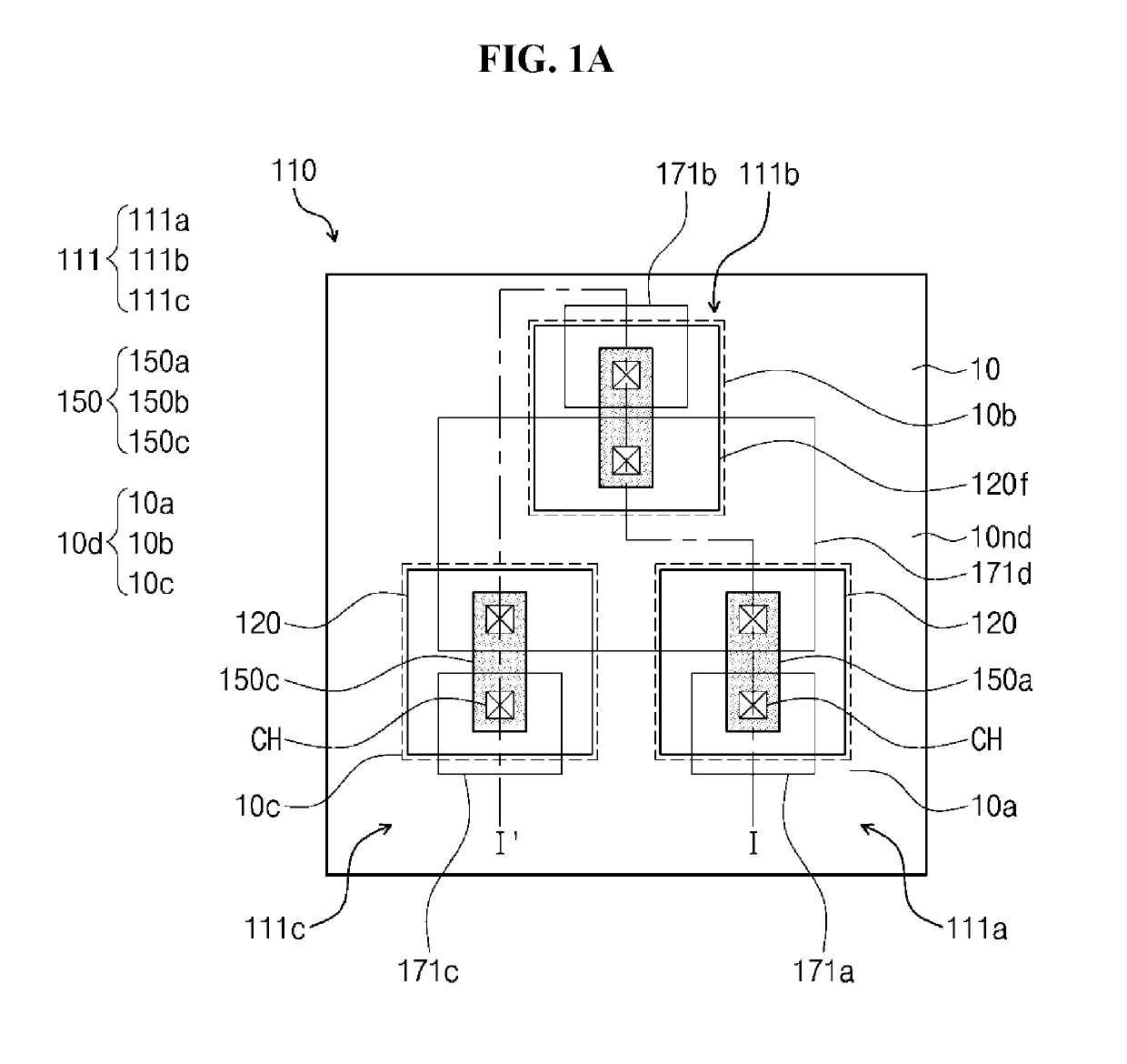
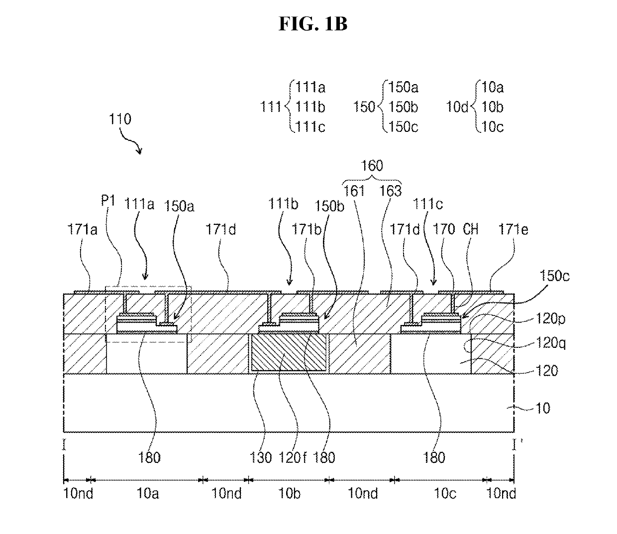
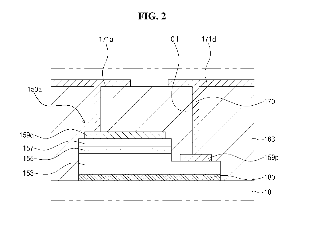
[0054]In the following description, for the purposes of explanation, numerous specific details are set forth in order to provide a thorough understanding of various exemplary embodiments or implementations of the invention. As used herein “embodiments” and “implementations” are interchangeable words that are non-limiting examples of devices or methods employing one or more of the inventive concepts disclosed herein. It is apparent, however, that various exemplary embodiments may be practiced without these specific details or with one or more equivalent arrangements. In other instances, well-known structures and devices are shown in block diagram form in order to avoid unnecessarily obscuring various exemplary embodiments. Further, various exemplary embodiments may be different, but do not have to be exclusive. For example, specific shapes, configurations, and characteristics of an exemplary embodiment may be used or implemented in another exemplary embodiment without departing from ...


PUM


Abstract

A displaying apparatus including: a panel substrate; a plurality of light emitting devices arranged on the panel substrate; and at least one connection tip disposed on one surface of each of the light emitting devices. Each of the light emitting devices includes a light emitting structure including a first conductivity type semiconductor layer, a second conductivity type semiconductor layer, and an active layer interposed between the first and second conductivity type semiconductor layers; and first and second electrode pads disposed on the light emitting structure.

Description

CROSS-REFERENCE TO RELATED APPLICATIONS[0001]This application claims priority from and the benefit of U.S. Provisional Application No. 62 / 595,010, filed on Dec. 5, 2017, U.S. Provisional Application No. 62 / 610,489, filed on Dec. 26, 2017, and U.S. Provisional Application No. 62 / 694,353, filed on Jul. 5, 2018, which are hereby incorporated by reference for all purposes as if fully set forth herein.BACKGROUNDField[0002]Exemplary embodiments of the invention relate generally to a displaying is apparatus having light emitting devices, a method of manufacturing the same, and a method of transferring light emitting devices.Discussion of the Background[0003]Light emitting devices are semiconductor devices using light emitting diodes which are inorganic light sources, and are used in various fields such as displaying apparatuses, automobile lamps, general lighting, and the like. Light emitting diodes have advantages such as long lifespan, low power consumption, and rapid response, and thus ...

Claims


Application Information

Patent Timeline
Patent Type & Authority Applications(United States)
IPC IPC(8): H01L25/075H01L33/00H01L25/16
CPCH01L25/0753H01L33/0079H01L25/167H01L27/156H01L21/6835H01L33/504H01L33/60H01L33/62H01L2933/0041H01L2933/0058H01L2933/0066H01L2221/68368H01L2221/68354H01L2221/68381H01L2221/68377H01L33/0093
Inventor TAKEYA, MOTONOBUSON, SEONG SULEE, JONG IKLIM, JAE HEECHAE, JONG HYEONHONG, SEUNG SIK
Owner SEOUL SEMICONDUCTOR
Why Eureka
Try Eureka