
Photoelectric sensor, photoelectric sensor module, and biological information measurement apparatus

Inactive Publication Date: 2019-08-01
SEIKO EPSON CORP
View PDF0 Cites 0 Cited by
  • Summary
  • Abstract
  • Description
  • Claims
  • Application Information

AI Technical Summary

Benefits of technology

This patent describes a photoelectric sensor that has a reduced thickness and complexity compared to traditional packaged LED chips and photodiodes. By using a silicon substrate and integrating the light emitter, light receiver, and control terminals, the sensor can be made thinner and more cost-effective. Additionally, the sensor can be easily integrated with other biological information measurement devices, increasing versatility and accuracy. The overall technical effects are improved accuracy and efficiency of biological information measurements.

Problems solved by technology

When the thickness of the sensor increases as described above, however, the thickness of a housing that accommodates the sensor tends to increase, resulting in a problem of poor usability felt by the user.

Method used


Image

  • Photoelectric sensor, photoelectric sensor module, and biological information measurement apparatus
  • Photoelectric sensor, photoelectric sensor module, and biological information measurement apparatus
  • Photoelectric sensor, photoelectric sensor module, and biological information measurement apparatus

Examples


first embodiment

[0058]A first embodiment of the invention will be described below with reference to the drawings.

[0059]Schematic configuration of biological information measurement apparatus

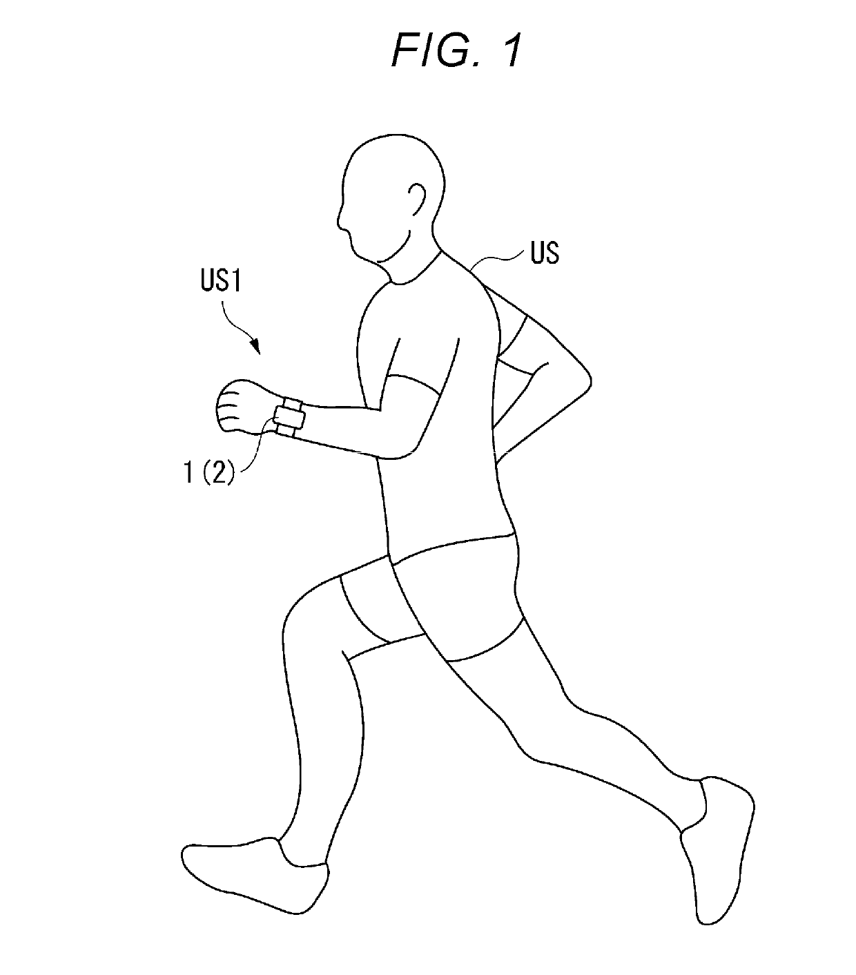
[0060]FIG. 1 is a diagrammatic view showing an example of how to use a biological information measurement apparatus 1 according to the present embodiment.

[0061]The biological information measurement apparatus 1 according to the present embodiment (hereinafter abbreviated to measurement apparatus 1 in some cases) is a wearable apparatus that is worn on the body of a user US when used, as shown in FIG. 1, and measures biological information associated with the user US. Specifically, the measurement apparatus 1 is worn on an apparatus worn site US1, such as a wrist of the user US, when used, detects the pulse wave of the user US as the biological information, and measures the pulse rate, which is also the biological information.

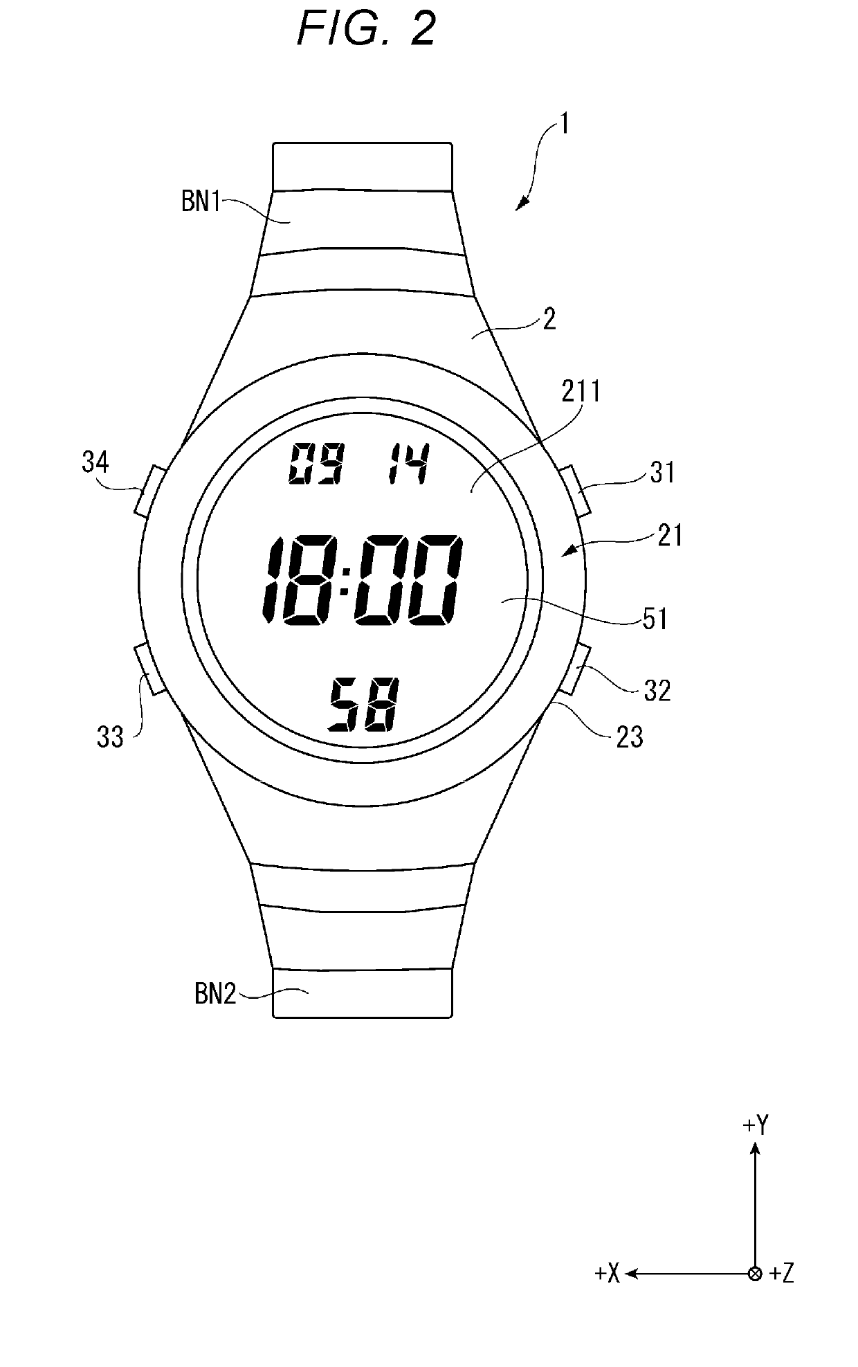
[0062]FIG. 2 shows the exterior appearance of the measurement apparatus 1.

[0063]The meas...

second embodiment

[0179]A second embodiment of the invention will next be described.

[0180]A biological information measurement apparatus according to the present embodiment has a configuration similar to that of the biological information measurement apparatus 1 shown in the first embodiment but differs from the biological information measurement apparatus 1 in that the photoelectric sensor further includes a light blocker disposed between the light emitter 822 and the light receiver 824. In the following description, the same or roughly the same portions as those having been already described have the same reference characters and will not be described.

[0181]FIG. 10 shows a photoelectric sensor 82B provided in the biological information measurement apparatus according to the present embodiment viewed from the light output side (+Z-direction side). In FIG. 10, part of the configuration of the photoelectric sensor 82B is omitted.

[0182]The biological information measurement apparatus according to the p...


PUM


Abstract

A photoelectric sensor includes a silicon substrate, a light emitter that emits first light, a light receiver that receives second light, a light emitter terminal that supplies the light emitter with electric power, and a light receiver terminal to which the light receiver outputs a signal, and the light emitter, the light receiver, the light emitter terminal, and the light receiver terminal are provided on the silicon substrate.

Description

CROSS-REFERENCES TO RELATED APPLICATIONS[0001]This application claims priority to Japanese Patent Application No. 2018-015683, filed on Jan. 31, 2018, the entirety of which is herein incorporated by reference.BACKGROUND1. Technical Field[0002]The present invention relates to a photoelectric sensor, a photoelectric sensor module, and a biological information measurement apparatus.2. Related Art[0003]There has been a known measurement apparatus capable of measuring biological information. As an example of the measurement apparatus, there is a known biological information measurement apparatus including a sensor unit formed of a light emitter that emits light to a target object and a light receiver that receives light from the target object and serving as a biological information measurement module (see JP-A-2016-123715, for example).[0004]In the biological information measurement apparatus described in JP-A-2016-123715, the light emitter and the light receiver are mounted on a substra...

Claims


Application Information

Patent Timeline
IPC IPC(8): A61B5/024H01L27/32
CPCA61B5/02427H01L27/3227A61B2562/0233A61B2562/166A61B2562/06A61B5/7435A61B5/743A61B5/681A61B2562/0238A61B5/0245A61B5/14532A61B5/14552H10K59/60
Inventor KANO, KAZUYUKI
Owner SEIKO EPSON CORP
Learn More