PLASMA ENHANCED ATOMIC LAYER DEPOSITION (PEALD) OF SiN USING SILICON-HYDROHALIDE PRECURSORS

a technology of silicon hydrohalide and atomic layer deposition, which is applied in the direction of coating, chemical vapor deposition coating, metallic material coating process, etc., can solve the problems of void formation in the gap-filling process, slower growth inside, and higher growth rate, so as to reduce or eliminate voids and seams, and high side-wall conformality

Active Publication Date: 2019-10-31
ASM IP HLDG BV
View PDF0 Cites 234 Cited by
  • Summary
  • Abstract
  • Description
  • Claims
  • Application Information

AI Technical Summary

Benefits of technology

[0006]The silicon nitride films deposited by the disclosed methods may have a high side-wall conformality and in some embodiments the silicon nitride film may be thicker at the bottom of the sidewall than at the top of the sidewall in a trench structure. In gap fill processes, the silicon nitride deposition processes can reduce or eliminate voids and seams.

Problems solved by technology

Silicon nitride (SiN) films deposited on three-dimensional structures by typical Plasma-Enhanced Atomic Layer Deposition (PEALD) processes may have a number of undesirable features, such as a low side-wall conformality and / or relatively poor step coverage, leading to problems such as the formation of voids in a gap-fill process.
The lack of side-wall conformality may result from a higher growth rate at the entrance of the trench or other feature, with slower growth inside due, at least in part, to non-uniform reactant exposure inside the trench.
A lack of conformality may also result from re-sputtering at the entrance of the trench during plasma treatment.

Method used


Image

  • PLASMA ENHANCED ATOMIC LAYER DEPOSITION (PEALD) OF SiN USING SILICON-HYDROHALIDE PRECURSORS
  • PLASMA ENHANCED ATOMIC LAYER DEPOSITION (PEALD) OF SiN USING SILICON-HYDROHALIDE PRECURSORS
  • PLASMA ENHANCED ATOMIC LAYER DEPOSITION (PEALD) OF SiN USING SILICON-HYDROHALIDE PRECURSORS

Examples


example

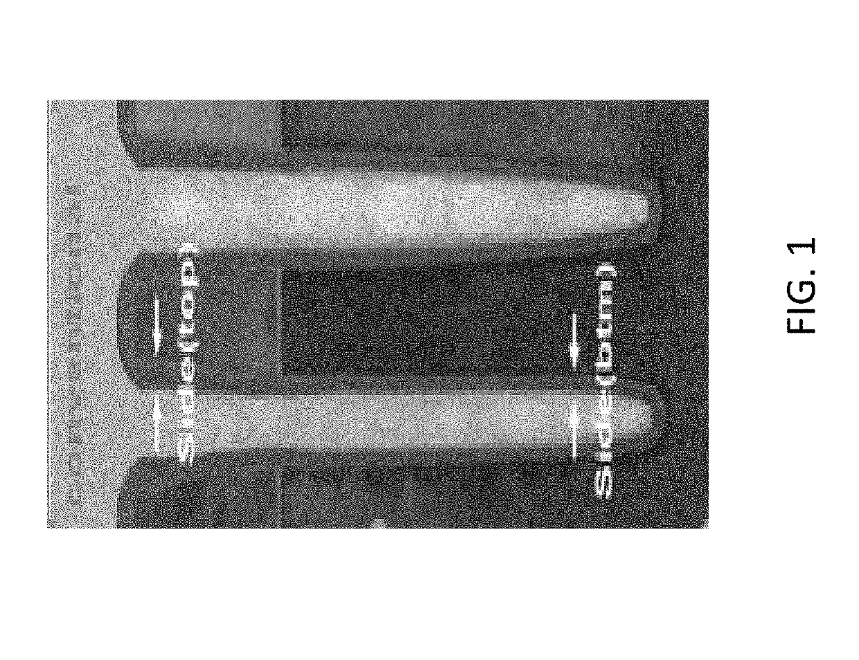
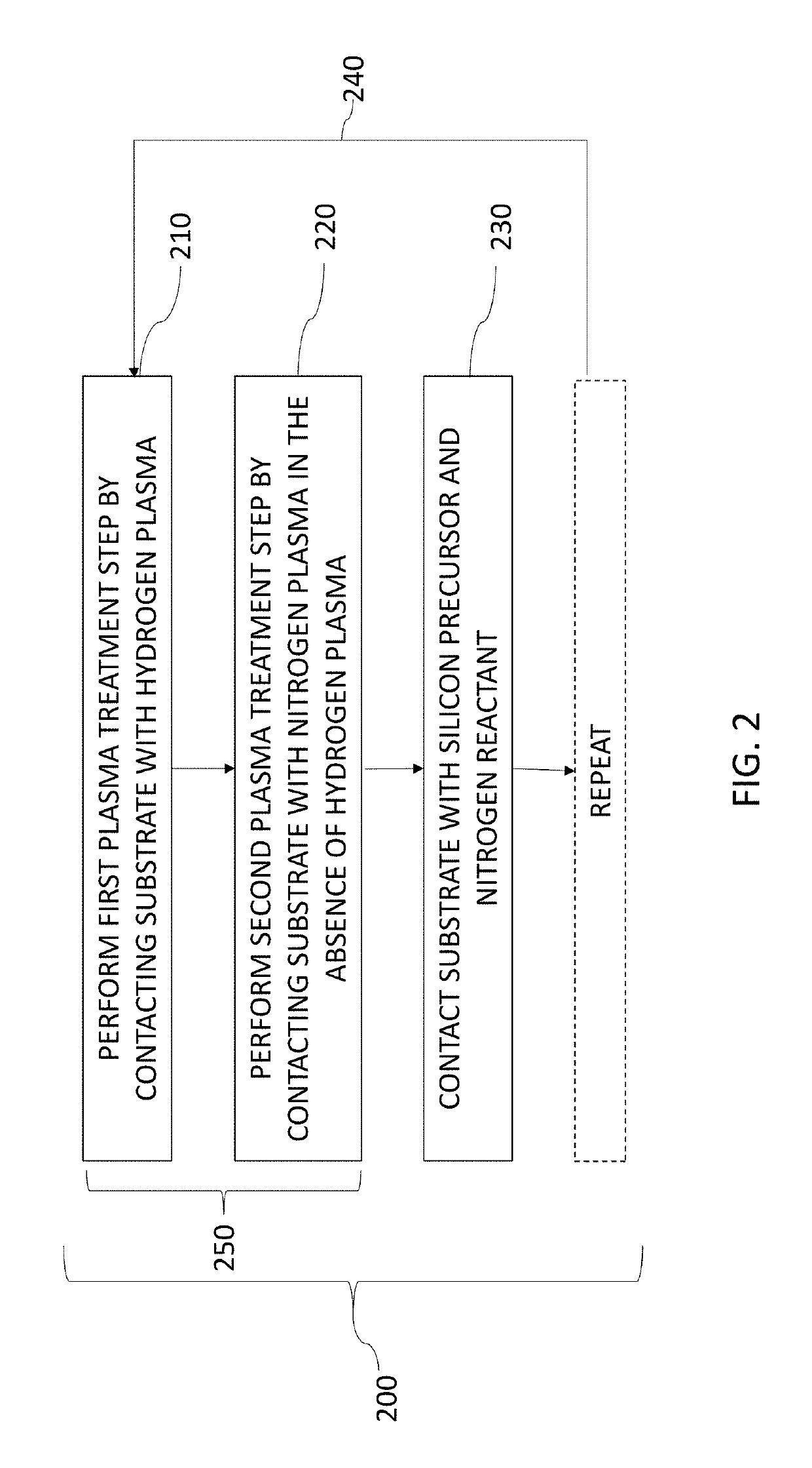
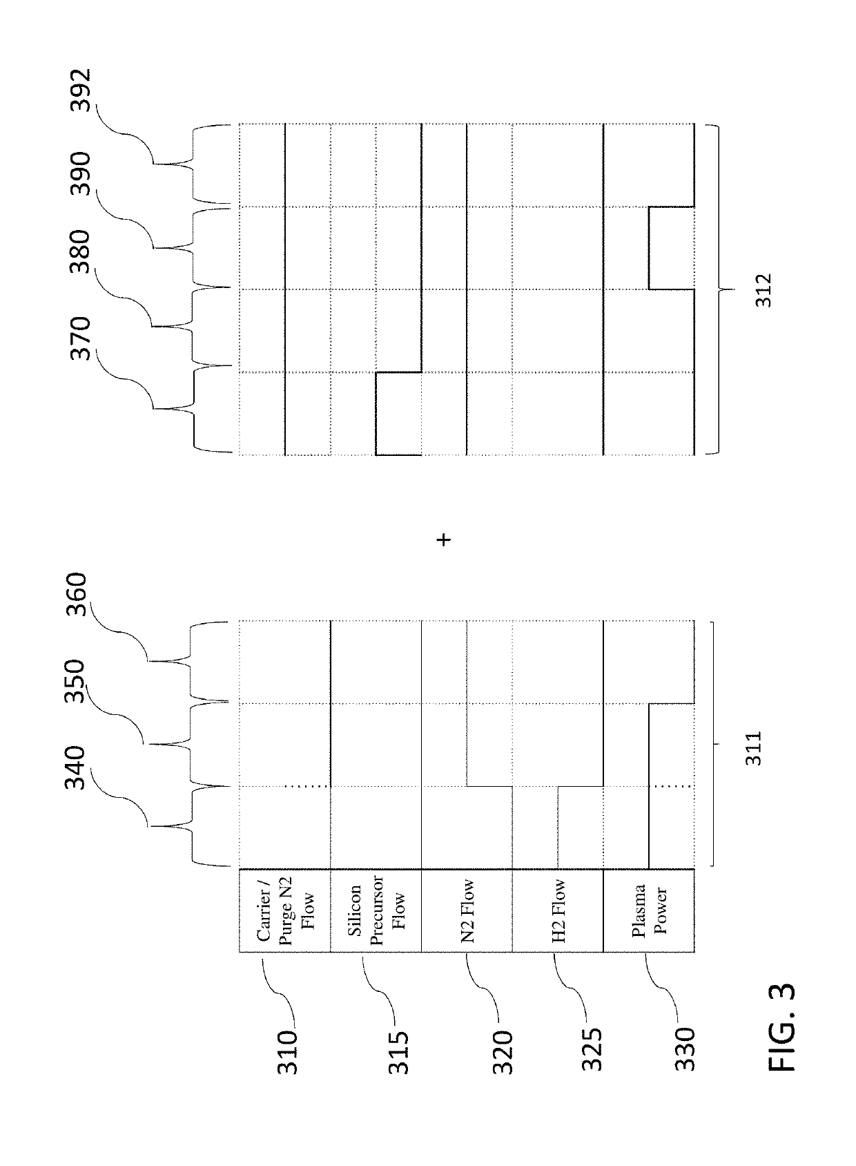
[0123]FIGS. 6A and 6B illustrate STEM images of SiN films deposited on structures having an AR of 10 according to some embodiments of the present disclosure. Sidewall conformality of >200% was obtained (FIG. 6A), and a structure with only a small seam is obtained in a gap fill process (FIG. 6B). Specifically, the SiN deposition was carried out at 400° C. while the reaction chamber was maintained at 2000 Pa (15 ton). A sequential plasma pretreatment phase comprised contacting the substrate simultaneously with a hydrogen and nitrogen plasma for 2 seconds, and subsequently contacting the substrate with a second nitrogen plasma in the absence of hydrogen plasma for 2 seconds. During the SiN deposition phase the substrate was contacted with a silicon precursor.


PUM

PropertyMeasurementUnit
aspect ratioaaaaaaaaaa

Abstract

Methods for forming silicon nitride films are provided. In some embodiments, silicon nitride can be deposited by atomic layer deposition (ALD), such as plasma enhanced ALD. One or more silicon nitride deposition cycle comprise a sequential plasma pretreatment phase in which the substrate is sequentially exposed to a hydrogen plasma and then to a nitrogen plasma in the absence of hydrogen plasma, and a deposition phase in which the substrate is exposed to a silicon precursor. In some embodiments a silicon hydrohalide precursors is used for depositing the silicon nitride. The silicon nitride films may have a high side-wall conformality and in some embodiments the silicon nitride film may be thicker at the bottom of the sidewall than at the top of the sidewall in a trench structure. In gap fill processes, the silicon nitride deposition processes can reduce or eliminate voids and seams.

Description

BACKGROUNDField[0001]The present disclosure relates generally to the field of semiconductor device manufacturing and, more particularly, to atomic layer deposition of silicon nitride films with hydrogen plasma and nitrogen plasma treatment steps.Description of the Related Art[0002]Silicon nitride (SiN) films deposited on three-dimensional structures by typical Plasma-Enhanced Atomic Layer Deposition (PEALD) processes may have a number of undesirable features, such as a low side-wall conformality and / or relatively poor step coverage, leading to problems such as the formation of voids in a gap-fill process. This is especially true when SiN is deposited by PEALD onto structures with high aspect ratios (AR). FIG. 1 illustrates a scanning transmission electron microscopy (STEM) image of a typical example of a silicon nitride film deposited by PEALD over a three-dimensional structure on substrate with an aspect ratio of 10 by conventional methods.[0003]The lack of side-wall conformality m...

Claims


Application Information

Patent Timeline
Patent Type & Authority Applications(United States)
IPC IPC(8): H01L21/02
CPCH01L21/02315H01L21/0217H01L21/0228C23C16/0245C23C16/345C23C16/513C23C16/45525H01L21/02274H01L21/02211H01L21/0337C23C16/45542C23C16/4554C23C16/45553C23C16/045
Inventor UEDA, SHINYAEBISUDANI, TAISHISUZUKI, TOSHIYA
Owner ASM IP HLDG BV
Why Eureka
Try Eureka