

Solid-State Lighting With A Control Gear Cascaded By A Luminaire
a control gear and luminaire technology, applied in emergency power supply arrangements, instruments, transportation and packaging, etc., can solve the problems of high total cost of ownership, incompatibility between ballast identification and replacement, and high cost of ownership for this approach, so as to reduce voltage ripple, reduce the noise of electromagnetic interference, and improve the effect of power factor
- Summary
- Abstract
- Description
- Claims
- Application Information
AI Technical Summary
Benefits of technology
Problems solved by technology
Method used
Image

Examples
Embodiment Construction
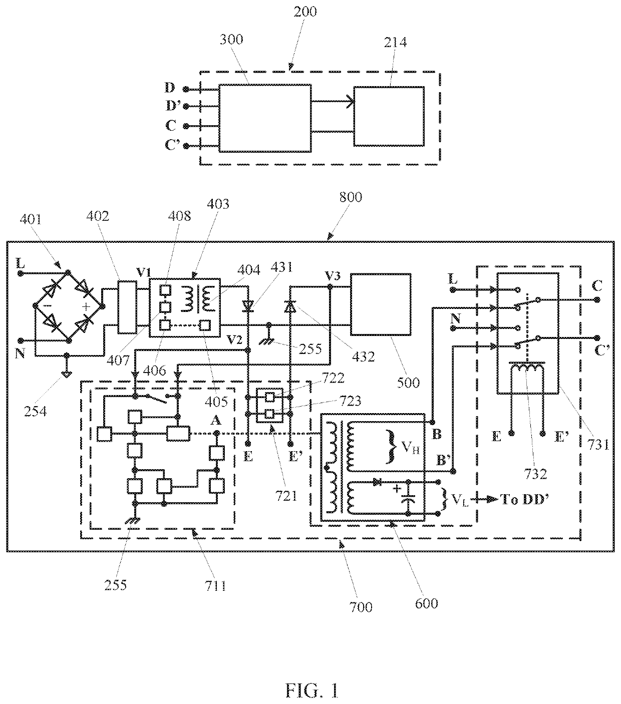
[0017]FIG. 1 is a block diagram of an LED luminaire control gear according to the present disclosure. The LED luminaire control gear 800 comprises a rechargeable battery 500, a full-wave rectifier 401, an input filter 402, a charging circuit 403, a current-fed inverter 600, and a line voltage detection and control circuit 700. In FIG. 1, the full-wave rectifier 401 is coupled to the AC mains and configured to convert the line voltage from the AC mains denoted as “L” and “N” into a first DC voltage, V1, after the input filter 402. The charging circuit 403 is an isolated step-down converter and comprises a first ground reference 254, a second ground reference 255 electrically isolated from the first ground reference 254, a transformer 404, a feedback control circuit 405, a control device 406, a first electronic switch 407, and a diode 408. The charging circuit 403 is coupled to the full-wave rectifier 401 via the input filter 402 and configured to convert the first DC voltage, V1, int...
PUM
 Abstract
Description
Claims
Application Information