Active learning for defect classifier training

a defect classifier and active learning technology, applied in the field of active learning for training a defect classifier, can solve the problems of difficult to find suitable examples, tedious and/or difficult nature of finding suitable examples, and difficulty in finding appropriate parameters,

Active Publication Date: 2019-12-05
KLA TENCOR TECH CORP
View PDF0 Cites 39 Cited by
  • Summary
  • Abstract
  • Description
  • Claims
  • Application Information

AI Technical Summary

Benefits of technology

[0014]Another embodiment relates to a non-transitory computer-readable medium storing program instructions executable on one or more computer systems for performing a computer-implemented method for performing active learning for training a defect classifier. The computer-implemented method includes the steps of the method described...

Problems solved by technology

However, as the dimensions of semiconductor devices decrease, inspection becomes even more important to the successful manufacture of acceptable semiconductor devices because smaller defects can cause the devices to fail.
One difficulty in finding appropriate parameters for an inspection process arises from the sometimes tedious and/or difficult nature of finding suitable examples of actual defects on a specimen that can be used to setup the inspection process.
Therefore, discovering DOIs and/or new DOI types may b...

Method used


Image

  • Active learning for defect classifier training
  • Active learning for defect classifier training
  • Active learning for defect classifier training

Examples


Embodiment Construction

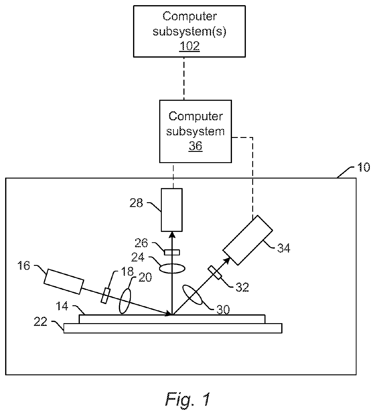
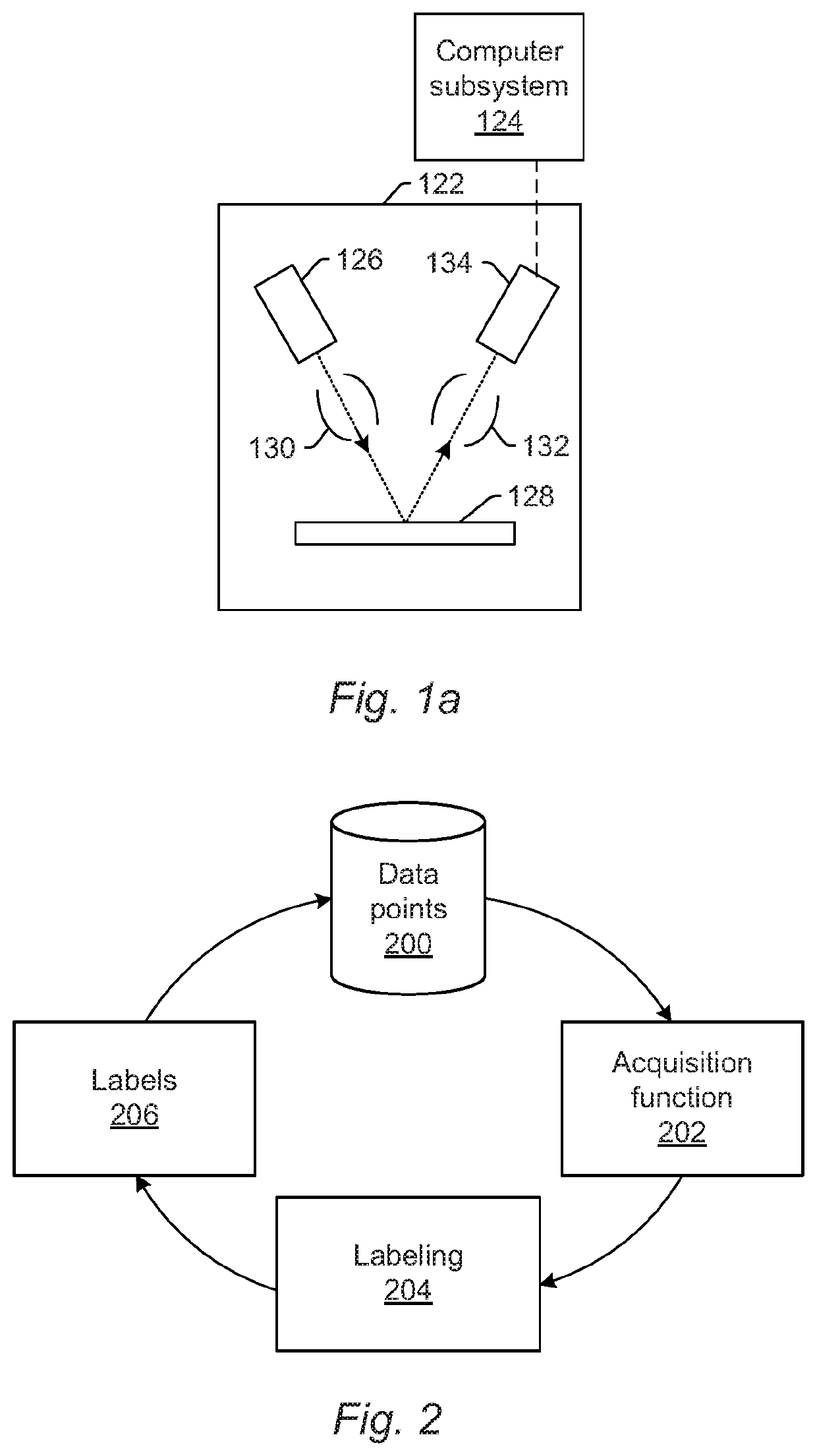
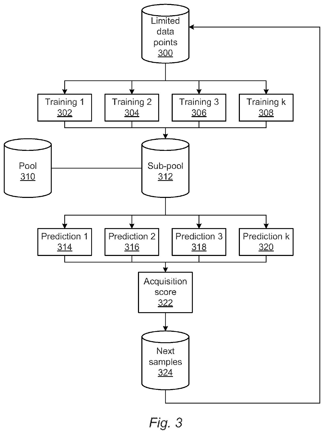
[0020]Turning now to the drawings, it is noted that the figures are not drawn to scale. In particular, the scale of some of the elements of the figures is greatly exaggerated to emphasize characteristics of the elements. It is also noted that the figures are not drawn to the same scale. Elements shown in more than one figure that may be similarly configured have been indicated using the same reference numerals. Unless otherwise noted herein, any of the elements described and shown may include any suitable commercially available elements.

[0021]One embodiment relates to a system configured to perform active learning for training a defect classifier. Some of the embodiments described herein are configured for Bayesian deep learning for adaptive sampling in semiconductor inspection and metrology applications.

[0022]Deep learning is considered a state-of-the-art solution to supervised learning when a sufficient amount of labeled data (on the order of millions) are economically available. ...


PUM


Abstract

Methods and systems for performing active learning for defect classifiers are provided. One system includes one or more computer subsystems configured for performing active learning for training a defect classifier. The active learning includes applying an acquisition function to data points for the specimen. The acquisition function selects one or more of the data points based on uncertainty estimations associated with the data points. The active learning also includes acquiring labels for the selected one or more data points and generating a set of labeled data that includes the selected one or more data points and the acquired labels. The computer subsystem(s) are also configured for training the defect classifier using the set of labeled data. The defect classifier is configured for classifying defects detected on the specimen using the images generated by the imaging subsystem.

Description

BACKGROUND OF THE INVENTION1. Field of the Invention[0001]The present invention generally relates to methods and systems for performing active learning for training a defect classifier.2. Description of the Related Art[0002]The following description and examples are not admitted to be prior art by virtue of their inclusion in this section.[0003]Fabricating semiconductor devices such as logic and memory devices typically includes processing a substrate such as a semiconductor wafer using a large number of semiconductor fabrication processes to form various features and multiple levels of the semiconductor devices. For example, lithography is a semiconductor fabrication process that involves transferring a pattern from a reticle to a resist arranged on a semiconductor wafer. Additional examples of semiconductor fabrication processes include, but are not limited to, chemical-mechanical polishing (CMP), etch, deposition, and ion implantation. Multiple semiconductor devices may be fabric...

Claims


Application Information

Patent Timeline
IPC IPC(8): G06T7/00G06N3/08G06N3/04G06K9/62G06N20/00G06F17/18G06N7/00
CPCG06N3/088G06N7/005G06K9/6253G06F17/18G06K9/628G06T7/0004G06N20/00G06N3/0472G06T2207/20081G06T2207/30148G06N3/08G06N7/01H01L21/67242H01L22/30H01L22/12H01L22/24G03F7/7065G03F7/70675G06F18/40G06F18/2431G06N3/047
Inventor ZHANG, JINGDONG, YUJIEDUFFY, BRIANWALLINGFORD, RICHARDDAINO, MICHAELBHASKAR, KRIS
Owner KLA TENCOR TECH CORP
Why Eureka
Try Eureka