Micro laser diode transfer method and manufacturing method

a technology manufacturing methods, which is applied in the direction of lasers, semiconductor lasers, electrical devices, etc., can solve the problems of not being suitable for the application of micro laser diodes, not being suitable for display devices using micro laser diodes, and not being suitable for projection displays

Active Publication Date: 2019-12-19
GOERTEK INC
View PDF55 Cites 0 Cited by
  • Summary
  • Abstract
  • Description
  • Claims
  • Application Information

AI Technical Summary

Benefits of technology

[0020]According to an embodiment of this invention, the present invention can provide a new approach for transferring micro laser diodes.

Problems solved by technology

They are not suitable for the application of a micro laser diode.
Furthermore, they are not suitable for a display device using micro laser diodes, especially, a high definition (HD) display device.
But, they are not suitable for projection display.
A projection display apparatus using micro-LEDs requires a complicated optical focusing system, which limits its application.

Method used


Image

  • Micro laser diode transfer method and manufacturing method
  • Micro laser diode transfer method and manufacturing method
  • Micro laser diode transfer method and manufacturing method

Examples


Embodiment Construction

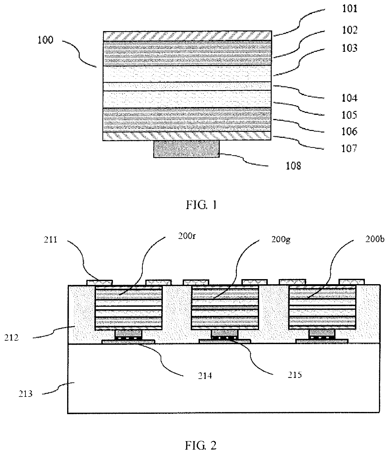
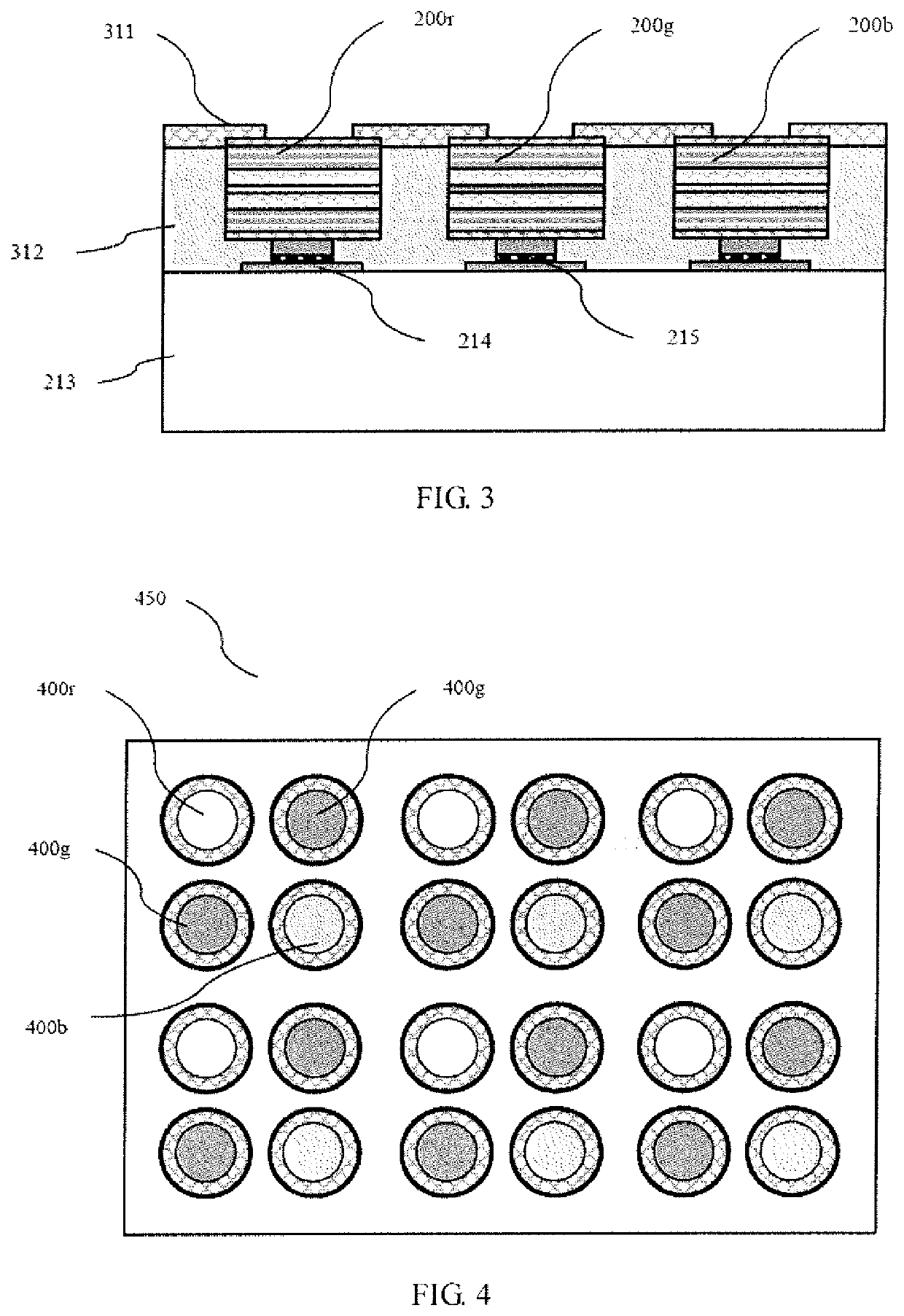
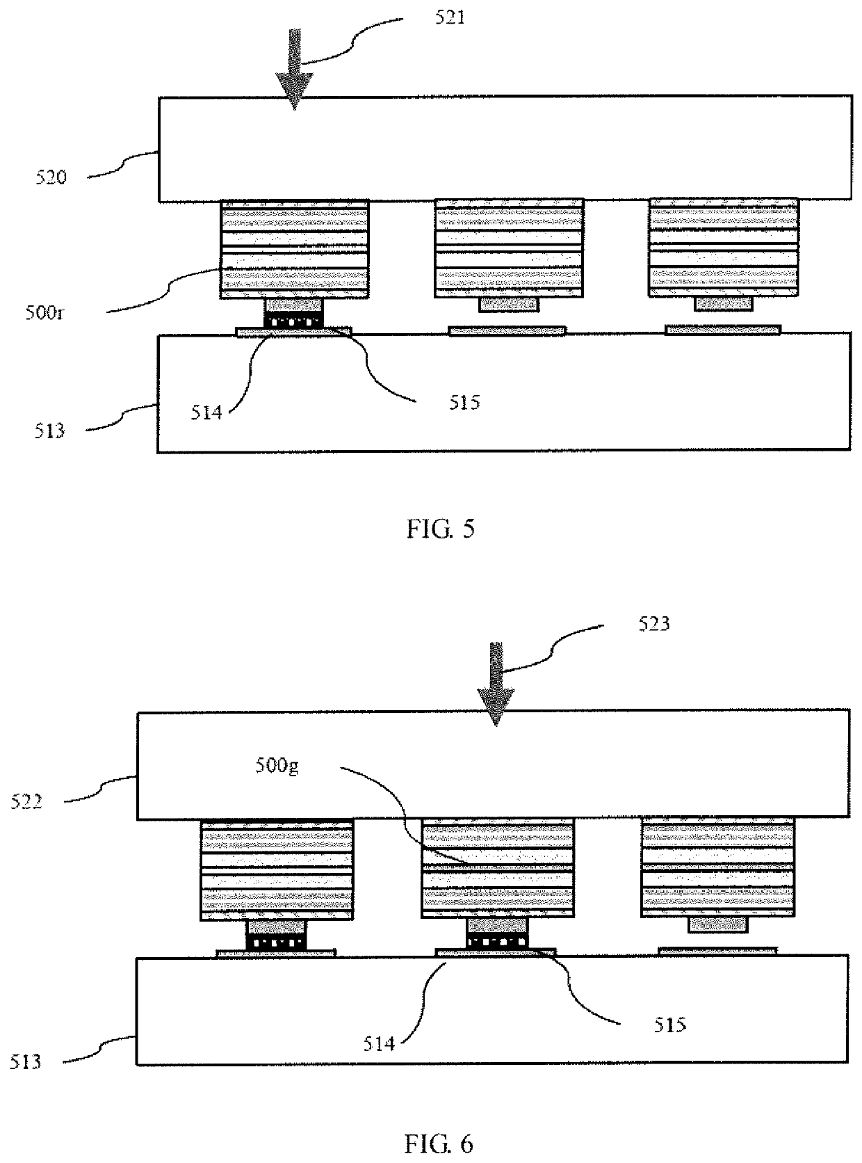
[0028]Various exemplary embodiments of the present invention will now be described in detail with reference to the drawings. It should be noted that the relative arrangement of the components and steps, the numerical expressions, and numerical values set forth in these embodiments do not limit the scope of the present invention unless it is specifically stated otherwise.

[0029]The following description of at least one exemplary embodiment is merely illustrative in nature and is in no way intended to limit the invention, its application, or uses.

[0030]Techniques, methods and apparatus as known by one of ordinary skill in the relevant art may not be discussed in detail but are intended to be part of the specification where appropriate.

[0031]In all of the examples illustrated and discussed herein, any specific values should be interpreted to be illustrative only and non-limiting. Thus, other examples of the exemplary embodiments could have different values.

[0032]Notice that similar refe...


PUM


Abstract

A micro laser diode transfer method and a manufacturing method comprise: forming a bonding layer (515) on a receiving substrate (513), wherein first type electrodes (514) are connected to the bonding layer (515); bringing a first side of the micro laser diodes (500r) on a carrier substrate (520) into contact with the bonding layer (515), wherein the carrier substrate (520) is laser-transparent; and irradiating selected micro laser diodes (500r) with laser from the side of the carrier substrate (520) to lift-off the selected micro laser diodes (500r) from the carrier substrate (520). This method may improve yield.

Description

CROSS-REFERENCE TO RELATED APPLICATIONS[0001]This application is a National Stage of International Application No. PCT / CN2016 / 108557 filed on Dec. 5, 2016, which is hereby incorporated by reference in its entirety.FIELD OF THE INVENTION[0002]The present invention relates to micro laser diode, and more specifically, to a method for transferring micro laser diodes and a method for manufacturing a micro laser diode device.BACKGROUND OF THE INVENTION[0003]The laser diode (LD) has been actively developed recently. Generally, a laser diode or a laser diode array is used as a light source for optical communications or a laser printer. The laser diode could be of a vertical cavity surface emitting laser (VCSEL) structure, which includes a lower contact layer, a lower Bragg reflector layer, a lower spacer layer, an active layer, an upper spacer layer, an upper Bragg reflector layer and an upper contact layer.[0004]In the prior art, micro laser diodes are transferred onto a receiving substrat...

Claims


Application Information

Patent Timeline
Patent Type & Authority Applications(United States)
IPC IPC(8): H01S5/02H01S5/183H01S5/042H01S5/0239
CPCH01S5/0216H01S5/18369H01S5/04256H01S5/022H01S5/4093H01S5/0217H01S5/183H01S5/0234H01S5/0237H01S5/0239H01S5/423
Inventor ZOU, QUANBOWANG, ZHE
Owner GOERTEK INC
Why Eureka
Try Eureka