Switching power supply device and semiconductor device

a technology of switching power supply and semiconductor, which is applied in the direction of electric variable regulation, process and machine control, instruments, etc., can solve the problems of difficult protection of output voltage, and achieve the effect of satisfying overvoltage protection

Active Publication Date: 2019-12-26
ROHM CO LTD
View PDF7 Cites 9 Cited by
  • Summary
  • Abstract
  • Description
  • Claims
  • Application Information

AI Technical Summary

Benefits of technology

[0023]According to the present invention, it is possible to provide a switching power supply device and a semiconductor device that contribute to the attainment of satisfactory overvoltage protection.

Problems solved by technology

Inconveniently, depending on the type of faults that can occur in switching power supply devices, it can be difficult to protect the output voltage from an overvoltage (details will be given later), and thus there is room for improvement in the overvoltage protection function.

Method used


Image

  • Switching power supply device and semiconductor device
  • Switching power supply device and semiconductor device
  • Switching power supply device and semiconductor device

Examples


first embodiment

[0042]A first embodiment of the present invention will be described. FIG. 1 is an overall configuration diagram of a switching power supply device 1 according to the first embodiment of the present invention. The switching power supply device 1 of FIG. 1 includes a switching power supply IC 100 and a plurality of discrete components that are externally connected to the switching power supply IC 100, and these discrete components include a capacitor C1, a coil L1, and resistors R1 and R2. The switching power supply device 1 is configured as a step-down switching power supply device that generates from a desired input voltage Vin a desired output voltage Vout. The output voltage Vout is supplied to a load LD, which is connected to an output terminal OUT. The input voltage Vin and the output voltage Vout are positive direct-current voltages, and the output voltage Vout is lower than the input voltage Vin. The output voltage Vout appears at the output terminal OUT of the switching power...

second embodiment

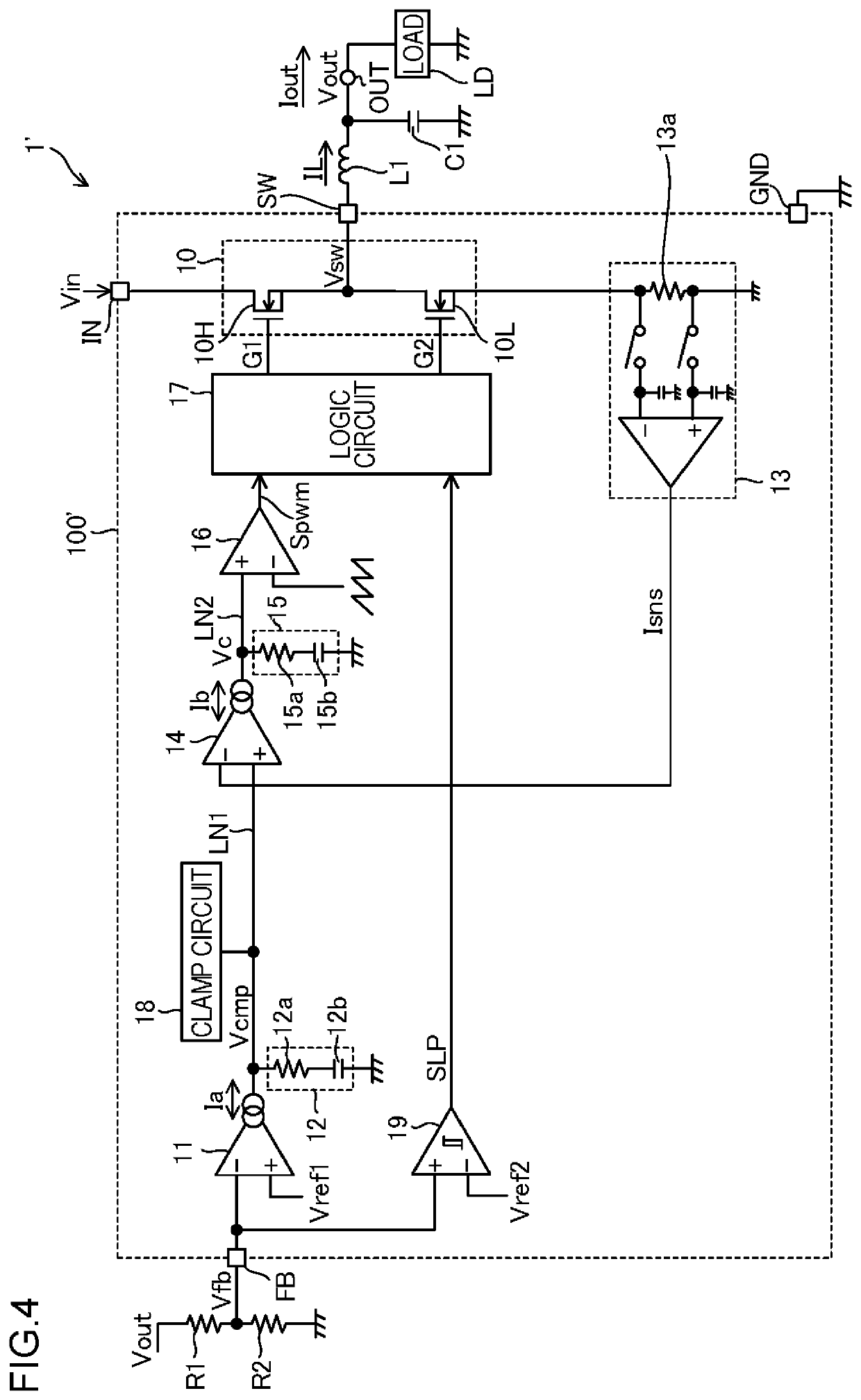
[0115]A second embodiment of the present invention will be described. The second embodiment is an embodiment based on the first embodiment. Accordingly, for those features of the second embodiment which are not specifically described, unless inconsistent, the corresponding description of the first embodiment applies to the second embodiment. For any description of the second embodiment that contradicts between the first and second embodiments, the description of the second embodiment prevails.

[0116]FIG. 11 is an overall configuration diagram of a switching power supply device 1A according to a second embodiment of the present invention. The switching power supply device 1A of FIG. 11 includes a switching power supply IC 100A and a plurality of discrete components that are externally connected to the switching power supply IC 100A, and these discrete components include a capacitor C1, a coil L1, and resistors R1 and R2.

[0117]In the IC 100A, compared with the IC 100 in FIG. 1, the cla...

third embodiment

[0124]A third embodiment of the present invention will be described. The third embodiment deals with techniques that can be implemented in combination with the first or second embodiment or modified techniques that can be applied to the first or second embodiment. The third embodiment includes Practical Examples EX3_1 to EX3 6 presented below, of which any one can be combined with any other.

Practical Example EX3_1

[0125]Practical Example EX3_1 will be described. FIG. 12A is an exterior view of a car navigation device 300 according to Practical Example EX3_1, and FIG. 12B is an outline configuration block diagram of the car navigation device 300. The car navigation device 300 includes a switching power supply device 301, a DC-DC converter 302, and a functional block 303. Used as the switching power supply device 301 is the switching power supply device 1 or 1A described previously. The input voltage Vin to the switching power supply device 301 can be supplied from a battery provided o...


PUM


Abstract

A switching power supply device has a switching output stage generating an output voltage from an input voltage by switching operation and a controller controlling the switching output stage based on a feedback voltage commensurate with the output voltage. The switching power supply device can perform switching suspension control whereby it stops switching operation on detecting a light-load condition based on the feedback voltage, though it restarts switching operation on detection of an overvoltage condition during suspension of switching operation.

Description

[0001]This nonprovisional application claims priority under 35 U.S.C. § 119(a) on Patent Application No. 2018-118504 filed in Japan on Jun. 22, 2018, the entire contents of which are hereby incorporated by reference.BACKGROUND OF THE INVENTION1. Field of the Invention[0002]The present invention relates to a switching power supply device and a semiconductor device.2. Description of Related Art[0003]There are generally known switching power supply devices that include an output transistor provided between a terminal to which an input voltage is applied and a terminal to which an output voltage is applied and that make the output transistor perform switching based on a feedback voltage commensurate with the output voltage and a predetermined reference voltage. For switching control, current-mode control is often adopted (see Patent Document 1 identified below).[0004]In switching power supply devices, protection of the output voltage from an overvoltage is essential, and hence many swit...

Claims


Application Information

Patent Timeline
Patent Type & Authority Applications(United States)
IPC IPC(8): H02M3/335H02H7/12
CPCH02M2001/0054H02M3/33592H02H7/1213H02M1/32H02M3/158H02M3/1588H02H7/0827H02H3/325H02H7/1227Y02B70/10H02M1/0032H02M1/0054H02M3/156
Inventor FUKUSHIMA, SHUNFUKUMOTO, YOSUKE
Owner ROHM CO LTD
Why Eureka
Try Eureka