Semiconductor package and manufacturing method thereof

a technology of semiconductors and packaging, applied in the direction of semiconductor devices, semiconductor/solid-state device details, electrical apparatus, etc., can solve the problems of increasing cross electromagnetic interference, reducing performance, and building up heat generated by components, so as to reduce electromagnetic interference and effectively dissipate heat

Active Publication Date: 2020-01-09
POWERTECH TECHNOLOGY
View PDF1 Cites 11 Cited by
  • Summary
  • Abstract
  • Description
  • Claims
  • Application Information

AI Technical Summary

Benefits of technology

[0003]The disclosure provides a semiconductor package and a manufacturing method thereof, and the semiconductor package is capable of effectively dissipating heat and reducing electromagnetic interference affecting a semiconductor die within the semiconductor package.
[0006]Based on the above, the conductive casing within the semiconductor package may effectively dissipate heat generated by the semiconductor die and other circuitry within the package. Moreover, the conductive casing may shield the semiconductor die from EMI. In addition, the first terminal penetrating through the redistribution structure to connect the conductive casing forms a direct path for transmitting electrical noise picked up by the conductive casing to ground. As a result, the performance of the semiconductor package may be further enhanced. The conductive connector provides for connecting further semiconductor packages disposed on the semiconductor package, and thereby enable package on package (PoP) stacked arrangements of semiconductor packages. As a result, the performance of PoP arrangements may also be further enhanced.

Problems solved by technology

The higher density of electronic components leads to a buildup of heat generated by the components, and the shorter distances between the semiconductor components leads to greater cross electromagnetic interference.
If not adequately addressed, both factors will lead to degradation in performance.
Therefore, continuing to miniaturize the semiconductor package while adequately dissipating heat and shielding from electromagnetic interference (EMI) in order to maintain a high performance of the semiconductor package and of the semiconductor die within the semiconductor package is a challenge to researchers in the field.

Method used


Image

  • Semiconductor package and manufacturing method thereof
  • Semiconductor package and manufacturing method thereof
  • Semiconductor package and manufacturing method thereof

Examples


Embodiment Construction

[0013]Reference will now be made in detail to the present preferred embodiments of the invention, examples of which are illustrated in the accompanying drawings. Wherever possible, the same reference numbers are used in the drawings and the description to refer to the same or like parts.

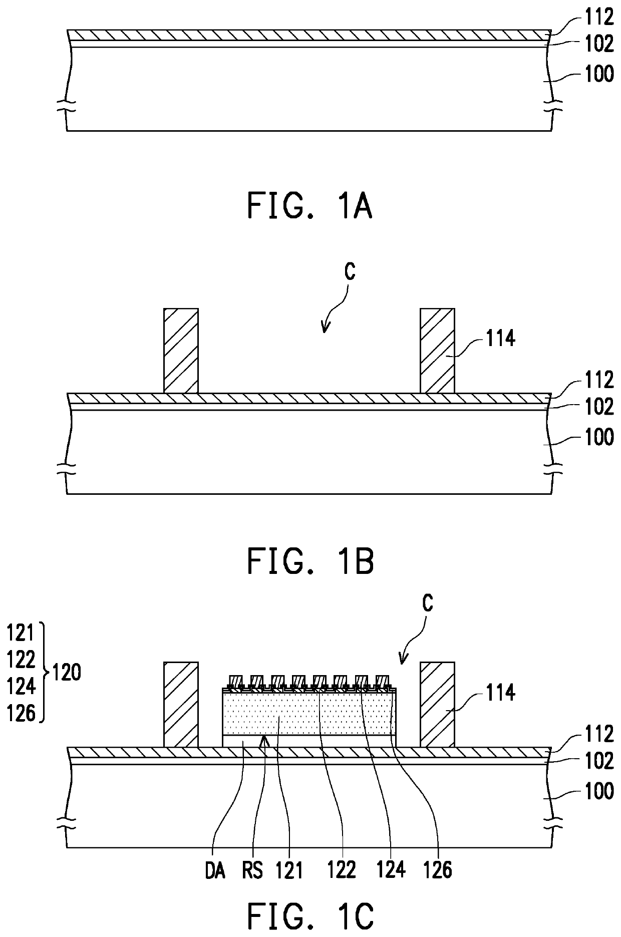
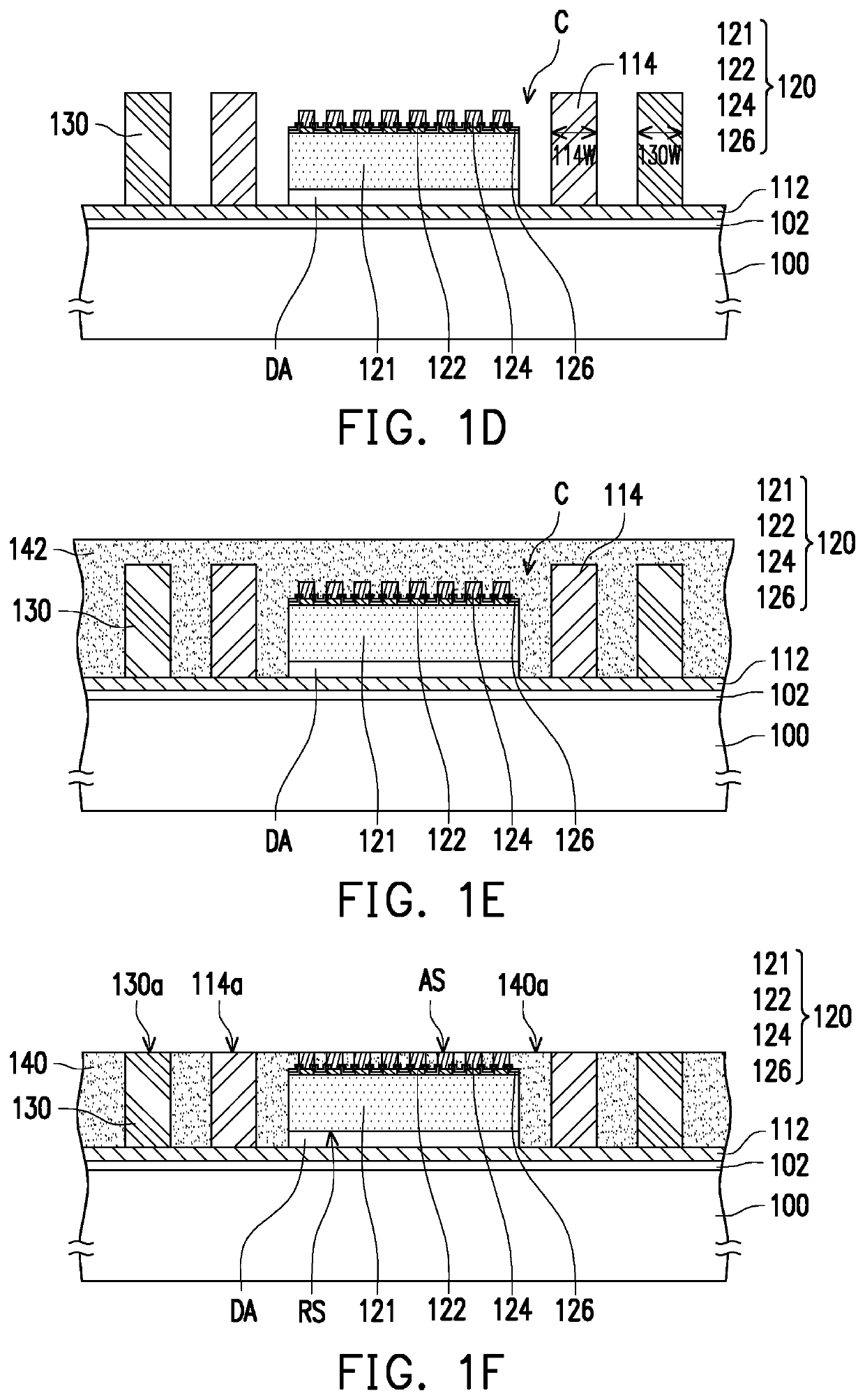
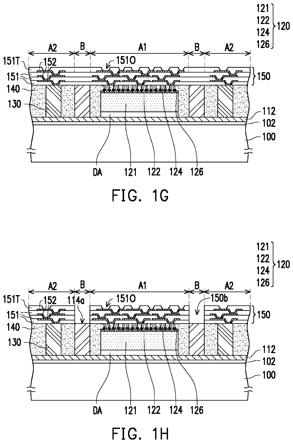
[0014]FIG. 1A to FIG. 1J are schematic cross-sectional views illustrating a manufacturing method of a semiconductor package 10 according to some embodiments of the disclosure, FIG. 2 is a schematic perspective top view of FIG. 1B, and FIG. 3 is a schematic top view of FIG. 1I. As shown in FIG. 1A, a temporary carrier 100 is provided. The temporary carrier 100 may be a substrate made of glass, plastic, metal, ceramic, or other suitable materials as long as the material is able to withstand the subsequent processes while carrying the package structure formed thereon.

[0015]In some embodiments, the temporary carrier 100 may be provided with a release layer 102 and a conductive layer 112 disposed thereon....


PUM

PropertyMeasurementUnit
conductiveaaaaaaaaaa
thicknessaaaaaaaaaa
heightaaaaaaaaaa

Abstract

A semiconductor package and a manufacturing method thereof are provided. The semiconductor package includes a conductive casing, a semiconductor die, a conductive connector, an insulating encapsulant, a redistribution structure, and a first conductive terminal. The conductive casing has a cavity. The semiconductor die is disposed in the cavity of the conductive casing. The conductive connector is disposed on a periphery of the conductive casing. The insulating encapsulant encapsulates the conductive connector, the semiconductor die and the cavity. The redistribution structure is formed on the insulating encapsulant and is electrically connected to the conductive connector and the semiconductor die. The first conductive terminal is disposed in openings of the redistribution structure and is physically in contact with a portion of the conductive casing.

Description

BACKGROUND OF THE INVENTIONField of the Invention[0001]The disclosure generally relates to a semiconductor package and a manufacturing method thereof, and in particular, to a semiconductor package having a conductive casing and a manufacturing method thereof.Description of Related Art[0002]Development of semiconductor package technology in recent years has focused on delivering smaller, more compact products with more densely packed components, resulting in shorter distances between semiconductor components. The higher density of electronic components leads to a buildup of heat generated by the components, and the shorter distances between the semiconductor components leads to greater cross electromagnetic interference. If not adequately addressed, both factors will lead to degradation in performance. Therefore, continuing to miniaturize the semiconductor package while adequately dissipating heat and shielding from electromagnetic interference (EMI) in order to maintain a high perfo...

Claims


Application Information

Patent Timeline
Patent Type & Authority Applications(United States)
IPC IPC(8): H01L23/538H01L23/13H01L23/31H01L23/00H01L21/56H01L25/10H01L25/00H01L23/367H01L23/552H01L21/683
CPCH01L2224/211H01L2221/68359H01L24/20H01L21/568H01L2224/32245H01L2224/83005H01L23/552H01L23/13H01L24/73H01L23/5389H01L21/6835H01L24/83H01L23/3128H01L2924/3025H01L24/32H01L2225/1094H01L2225/1035H01L25/105H01L25/50H01L2225/1058H01L23/3675H01L24/19H01L2224/73267H01L23/5386H01L2221/68381H01L23/49816H01L2221/68327H01L2221/68345H01L2224/18H01L2924/181H01L2924/00012
Inventor CHIANG, CHIA-WEIFANG, LI-CHIHFAN, WEN-JENG
Owner POWERTECH TECHNOLOGY
Why Eureka
Try Eureka