

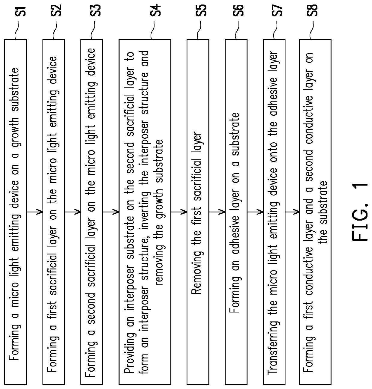
Light emitting device and manufacturing method thereof
a technology of light emitting devices and manufacturing methods, which is applied in the manufacture of semiconductor/solid-state devices, semiconductor devices, electrical devices, etc., can solve the problems of too small effective light-emitting area of micro light-emitting devices (leds), and achieve the effect of increasing the effective light-emitting area
- Summary
- Abstract
- Description
- Claims
- Application Information
AI Technical Summary
Benefits of technology
Problems solved by technology
Method used
Image

Examples
first embodiment
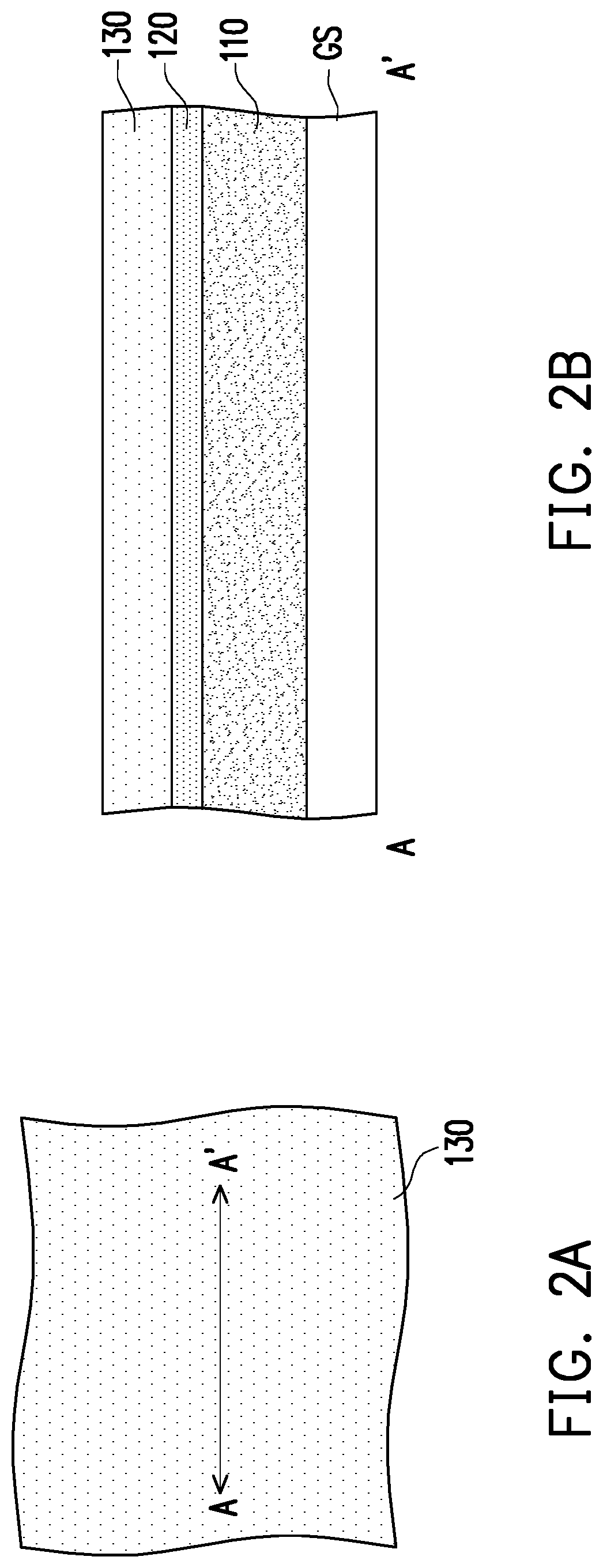
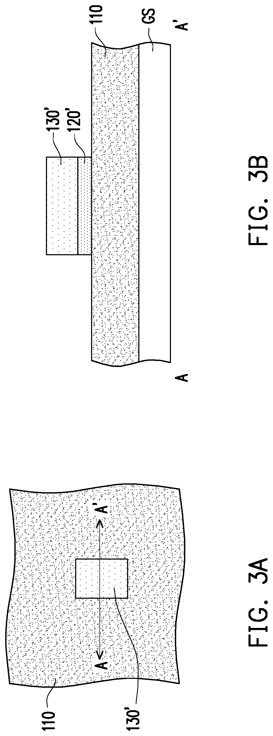
[0025]FIGS. 2A to 7A, 2B to 7B, and 7C are schematic views showing a method of forming a μLED on a growth substrate in the disclosure, wherein FIGS. 2B to 7B are schematic cross-sectional views taken along line AA′ of FIGS. 2A to 7A, and FIG. 7C is a schematic cross-sectional view taken along line BB′ of FIG. 7A.
[0026]Referring to FIG. 2A and FIG. 2B, a first semiconductor material layer 110, a light emitting material layer 120, and a second semiconductor material layer 130 are formed sequentially on the growth substrate GS as an example, but not limited to this. In other embodiments, the second semiconductor material layer 130, the light emitting material layer 120, and the first semiconductor material layer 110 are sequentially formed on the growth substrate GS. In other words, the first semiconductor material layer 110, the light emitting material layer 120, and the second semiconductor material layer 130 are formed on the growth substrate GS. The growth substrate GS may be a gal...
second embodiment
[0067]Referring to FIG. 18, in the light emitting device 20 of the second embodiment, a portion of the second extension portion 144′ is still substantially flush with the upper surface 310A of the adhesive layer 310 after the etching process (for example: the etching process of FIGS. 16A, 16B, and 16C). In other words, the second extension portion 144′ may still completely cover the side surface of the first semiconductor layer 110′ closing to the second electrode 154 after the etching process. The “substantially flush” can be means an upper surface of the portion of the second extension portion 144′ is substantially aligned with the upper surface 310A of the adhesive layer 310. In other words, a height of the portion of the second extension portion 144′ is substantially equal to a height of the upper surface 310A of the adhesive layer 310. The portion of the tether layer 140′ is located between the second conductive layer 164 and the first semiconductor layer 110′, thereby, a short...
fourth embodiment
[0075]Referring to FIG. 21, in a light emitting device 40 of the fourth embodiment, a first sub-groove 312A and a second sub-groove 312B are formed in the adhesive layer 310. A first conductive layer 162 and a second conductive layer 164 are formed respectively in the first sub-groove 312A and the second sub-groove 312B, wherein the first conductive layer 162 is in contact with the first pad 322 of the substrate RS, and the second conductive layer 164 is in contact with the second pad 324 of the substrate RS.
[0076]After forming the first conductive layer 162 and the second conductive layer 164, the micro light emitting device 100 is transferred onto the adhesive layer 310. The first electrode 152 is electrically connected to the first conductive layer 162, the second electrode 154 is electrically connected to the second conductive layer 164.
[0077]At least one of the first conductive layer 162 and the second conductive layer 164 may be a single layer or a multilayer structure, and th...
PUM
| Property | Measurement | Unit |
|---|---|---|
| width W1 | aaaaa | aaaaa |
| width W2 | aaaaa | aaaaa |
| size | aaaaa | aaaaa |
Abstract
Description
Claims
Application Information