Organic light emitting display panel, method of manufacturing same, and organic light emitting display device

A light-emitting display and manufacturing method technology, which is applied in semiconductor/solid-state device manufacturing, semiconductor devices, electrical components, etc., can solve the problems of parallax and low brightness of the camera area under the screen, so as to improve the sense of experience, solve the problem of parallax, and improve the photoelectricity. The effect of performance and brightness

Pending Publication Date: 2022-07-29
EVERDISPLAY OPTRONICS (SHANGHAI) CO LTD
View PDF0 Cites 1 Cited by
  • Summary
  • Abstract
  • Description
  • Claims
  • Application Information

AI Technical Summary

Problems solved by technology

[0005] In view of this, the present application provides an organic light-emitting display panel and its manufacturing method and an organic light-emitting display device to solve the parallax problem caused by the lower brightness of the camera area under the screen than other display areas in the prior art

Method used


Image

  • Organic light emitting display panel, method of manufacturing same, and organic light emitting display device
  • Organic light emitting display panel, method of manufacturing same, and organic light emitting display device
  • Organic light emitting display panel, method of manufacturing same, and organic light emitting display device

Examples


Embodiment Construction

[0040] Example embodiments will now be described more fully with reference to the accompanying drawings. However, example embodiments can be embodied in various forms and should not be construed as limited to the embodiments set forth herein. Rather, these embodiments are provided so that this application will be thorough and complete, and will fully convey the concept of example embodiments to those skilled in the art. The same reference numerals in the drawings denote the same or similar structures, and thus their repeated descriptions will be omitted.

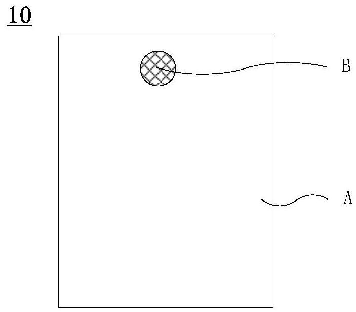
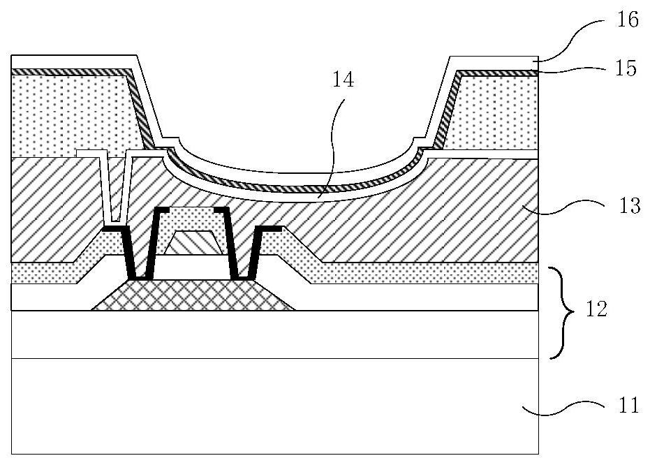
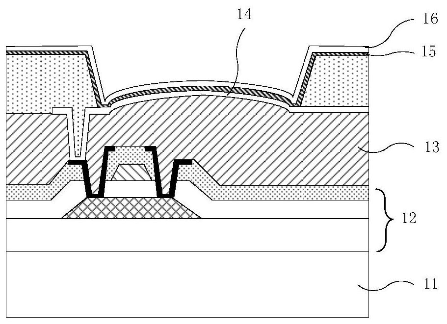
[0041] Please refer to figure 1 and figure 2 , which is a schematic structural diagram of an organic light-emitting display panel according to an embodiment of the present invention. like figure 1 and figure 2 As shown, the organic light emitting display panel 10 includes: a display area A and an imaging area B; both the imaging area B and the display area A include a base substrate 11 and a plurality of pixel units,...


PUM


Abstract

The invention provides an organic light-emitting display panel, a manufacturing method thereof and an organic light-emitting display device, and the organic light-emitting display panel comprises a display region and a camera region. Each of the camera shooting area and the display area comprises a substrate and a plurality of pixel units formed on the substrate, and an organic light emitting diode of each pixel unit comprises a stacked structure formed by an anode, an organic light emitting layer and a cathode; in the camera shooting area, the stacked structure of at least one organic light-emitting diode is a curved surface structure or a wave structure, and the curved surface structure faces the substrate or is opposite to the substrate. According to the organic light-emitting display panel, the manufacturing method thereof and the organic light-emitting display device, the OLED device in the camera shooting area is designed to be of the curved surface structure or the wave structure, so that the effective light-emitting area is increased, the photoelectric performance and the brightness of the OLED device in the camera shooting area are improved, the parallax problem is solved, and the user experience is improved.

Description

technical field [0001] The present application relates to the field of display technology, and in particular, to an organic light-emitting display panel, a method for manufacturing the same, and an organic light-emitting display device. Background technique [0002] Compared with many display devices, Organic Light Emitting Display (OLED) has all-solid-state, self-luminous, wide viewing angle, wide color gamut, fast response, high luminous efficiency, high brightness, high contrast, ultra-thin With many advantages such as ultra-light, low power consumption, wide operating temperature range, large-size and flexible panels, and simple manufacturing process, it can realize flexible display in the true sense and best meet people's requirements for future displays. [0003] At present, OLED display panels are developing towards a high screen-to-body ratio, and technologies such as flowing sea screens, water drop screens, and full-screen (that is, using an under-screen camera) hav...

Claims


Application Information

Patent Timeline
Patent Type & Authority Applications(China)
IPC IPC(8): H01L27/32H01L21/77
CPCH10K59/65H10K59/121H10K59/1201
Inventor 邹美玲
Owner EVERDISPLAY OPTRONICS (SHANGHAI) CO LTD
Why Eureka
Try Eureka