

Method of transferring device layer to transfer substrate and highly thermal conductive substrate
a transfer substrate and substrate technology, applied in the direction of semiconductor devices, basic electric elements, electrical appliances, etc., can solve the problems of heat dissipation, efficiency is favorable, heat dissipation, etc., and achieve high thermal conductive substrate, excellent heat dissipation property, and small loss
- Summary
- Abstract
- Description
- Claims
- Application Information
AI Technical Summary
Benefits of technology
Problems solved by technology
Method used
Image

Examples
example 1
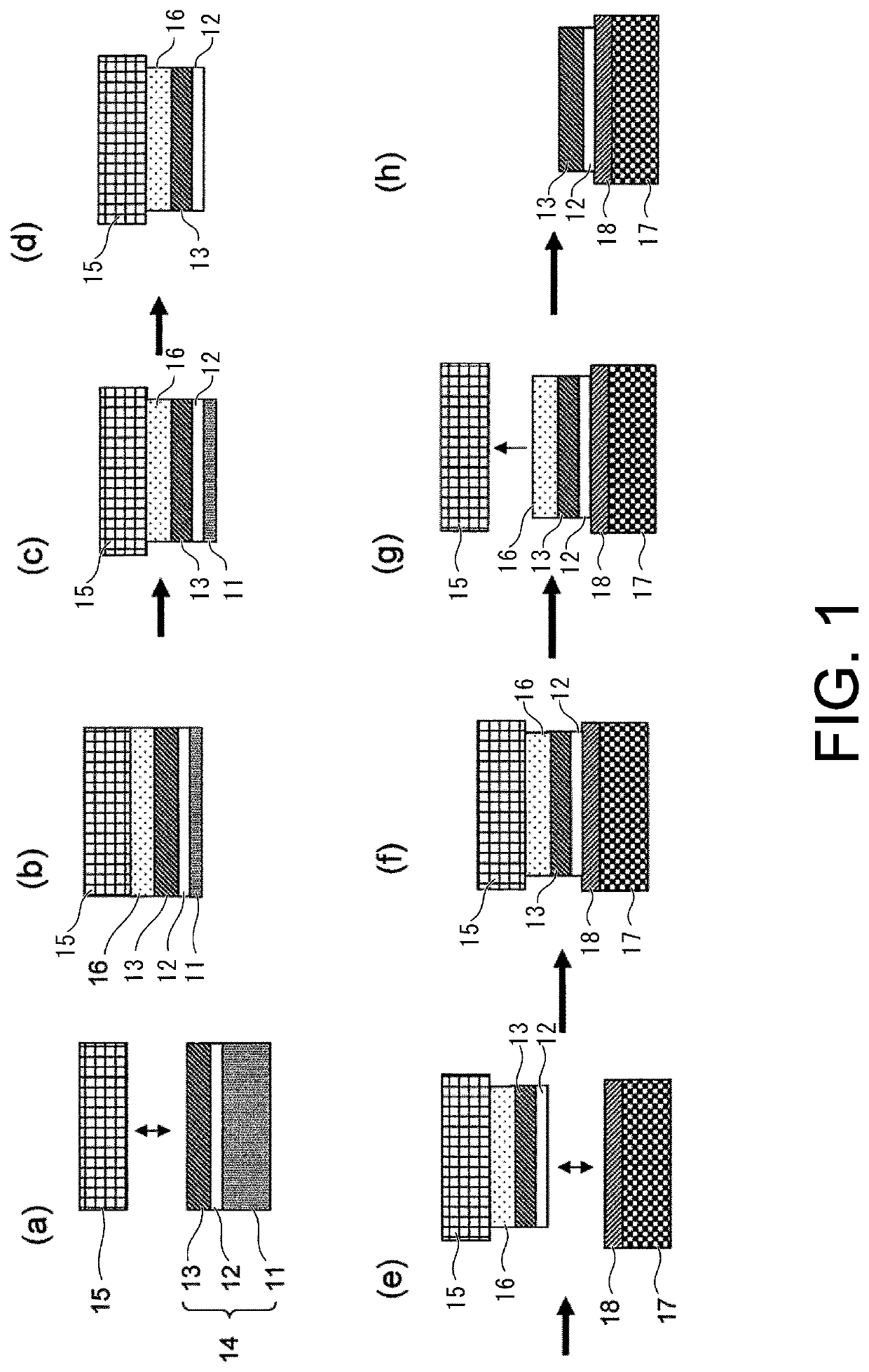
[0039]As the device wafer (SOI wafer) 14 on which a device was formed, a wafer which had an external form of 200 mm p and in which the thickness of the device layer 13 was 4 μm, the thickness of the buried oxide film 12 was 250 nm, and the thickness of the substrate (Si layer 11) was 725 μm was used. Solder bumps having a diameter of 80 μm were formed on the outermost surface of the device at a minimum pitch of 150 μm.
[0040]TA1070T / TA2570V3 / TA4070 which was an adhesive manufactured by Shin-Etsu Chemical Co., Ltd. as an adhesive for temporary bonding 16 was laminated and applied on the surface (namely, the surface provided with the device layer 13) of this SOI wafer 14 by spin coating. First, TA1070 T as a device protecting layer was laminated by 10 μm, TA2570V3 as a layer to be a release surface of the supporting substrate 15 after processing was laminated by 7 μm, and TA4070 as an adhesive layer with the supporting substrate 15 was laminated by 90 μm. A Si wafer was used as the sup...
example 2
[0048]A device wafer (SOI wafer) on which the device layer 13 was formed and which was described in Example 1 was prepared and a temporarily bonded wafer from which the Si layer 11 on the back surface of the wafer had been completely removed was fabricated according to the same procedure as in Example 1. The Si3N4 substrate was also coated with the adhesive for transfer 18 according to the same procedure, and the load at the time of bonding was lowered to 1 kgf / cm2.
[0049]The wafer was bonded. It was possible to transfer the device layer 13 to the Si3N4 substrate when the supporting substrate 15 was peeled off. Peeling off and deformation of the bumps were not observed when the device layer 13 after being cleaned was observed under an optical microscope.
example 3
[0050]A device wafer on which the device layer 13 was formed and which was described in Example 1 was prepared and a temporarily bonded wafer from which the Si layer 11 on the back surface of the wafer had been completely removed was fabricated according to the same procedure as in Example 1. The Si3N4 substrate was also coated with the adhesive for transfer 18 according to the same procedure, and the load at the time of bonding was raised to 10 kgf / cm2.
[0051]The wafer was bonded. It was possible to transfer the device layer 13 to the Si3N4 substrate when the supporting substrate 15 was peeled off. Peeling off and deformation of the bumps were not observed when the device layer 13 after being cleaned was observed under an optical microscope.
PUM
| Property | Measurement | Unit |
|---|---|---|
| thickness | aaaaa | aaaaa |
| Young's modulus | aaaaa | aaaaa |
| thickness | aaaaa | aaaaa |
Abstract
Description
Claims
Application Information