Liquid crystal display device

a liquid crystal display and display device technology, applied in semiconductor devices, optics, instruments, etc., can solve the problems of reducing the aperture ratio of the panel, increasing the power consumption of the panel, and reducing the display properties of the liquid crystal display device such as the contrast ratio, so as to improve the white display luminance and excellent light utilization efficiency

Inactive Publication Date: 2020-02-27
SHARP KK
View PDF13 Cites 0 Cited by
  • Summary
  • Abstract
  • Description
  • Claims
  • Application Information

AI Technical Summary

Benefits of technology

[0022]The present invention can provide a liquid crystal display device excellent in light utilization efficiency and advantageous for improvement of white display luminance.

Problems solved by technology

An increase in the definition of a liquid crystal panel increases the area of the panel occupied by the gate lines, the source lines, and the like formed on the TFT substrate, and thus tends to reduce the aperture ratio of the panel.
Such a reduction in the aperture ratio thus leads to a reduction in display properties of the liquid crystal display device such as a contrast ratio.
Although increasing the luminance of the backlight can compensate for the reduction in the luminance of the liquid crystal panel, it increases the power consumption of the panel.
In a liquid crystal panel with a lower aperture ratio, more light from the backlight is absorbed by the gate lines, the source lines and other lines formed on the TFT substrate, leading to poor light utilization efficiency.
Such poor light utilization efficiency is a fundamental cause of an increase in the panel power consumption.

Method used


Image

  • Liquid crystal display device
  • Liquid crystal display device
  • Liquid crystal display device

Examples


embodiment 1

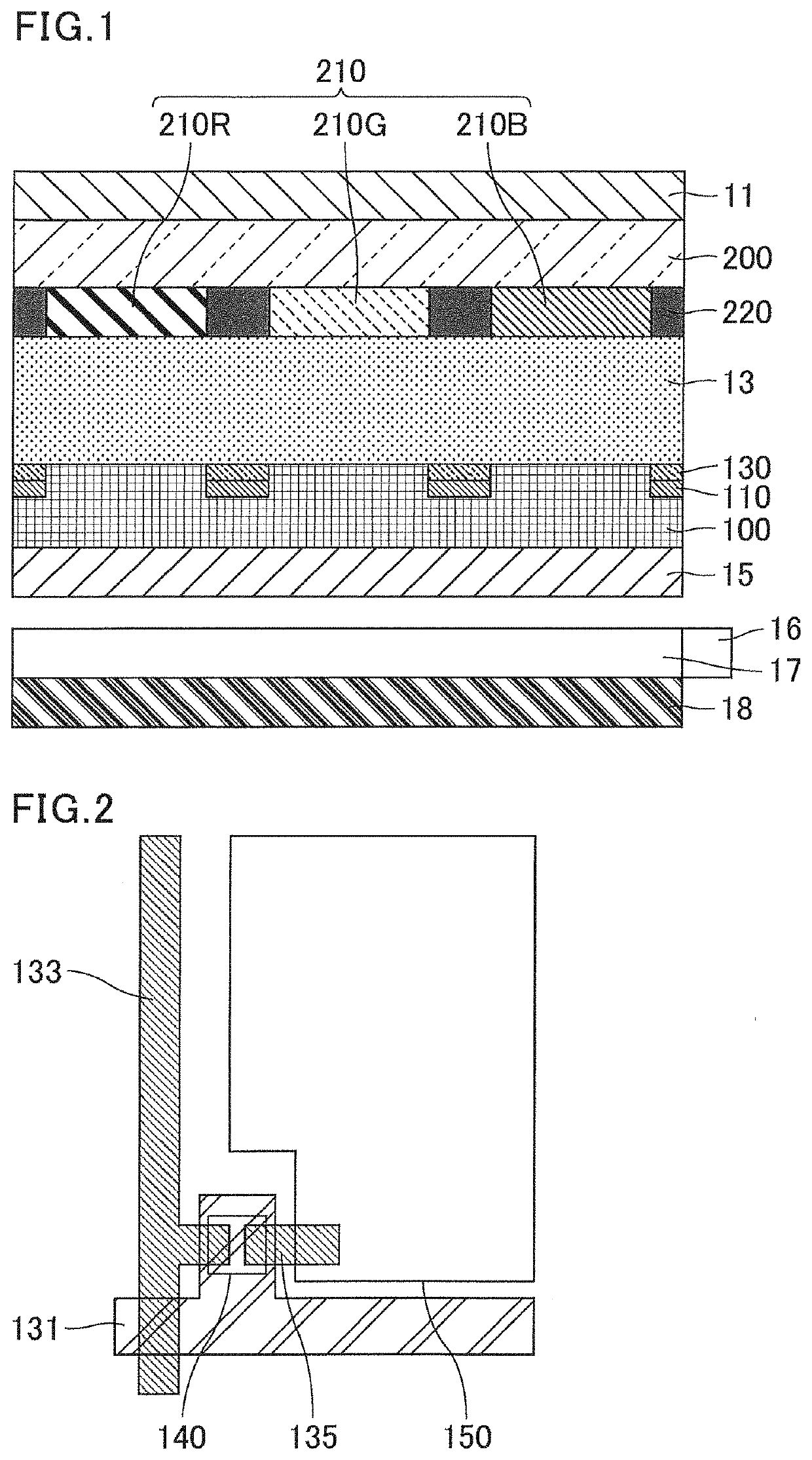
[0047]FIG. 1 is a schematic cross-sectional view illustrating the structure of a liquid crystal display device of Embodiment 1. As illustrated in FIG. 1, the liquid crystal display device of this embodiment includes a liquid crystal panel. The liquid crystal panel includes, in the order from the viewing surface side; a first polarizing plate 11; a color filter substrate (viewing surface side substrate) including a transparent substrate 200, a color filter (CF) layer 210, and a black matrix layer 220; a liquid crystal layer 13; a thin-film transistor substrate (back surface side substrate) including a transparent substrate 100, a reflective layer 110, and a line electrode layer 130; and a second polarizing plate 15. The color filter substrate and the thin-film transistor substrate are bonded to each other with a sealant surrounding the periphery of the liquid crystal layer 13. The liquid crystal layer 13 is held between the substrates.

[0048]A backlight is provided on the back surface...

embodiment 2

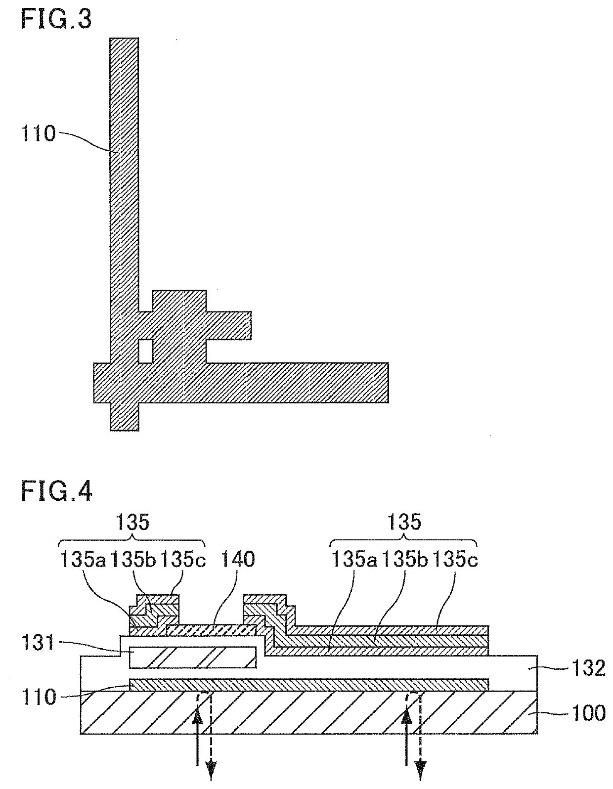
[0065]In the present invention, the reflective surface facing the backlight may be constituted by the gate electrode layer 131 constituted by a high reflectance material such as Al. In this case, the gate electrode layer 131 is disposed on the transparent substrate 100 side (backlight side) of the source electrode layer 133 and the drain electrode layer 135 to overlap the source electrode layer 133 and the drain electrode layer 135, and is electrically isolated from the source electrode layer 133 and the drain electrode layer 135.

[0066]FIG. 7 is a schematic plan view illustrating the structure of the gate electrode layer 131 of Embodiment 2. As illustrated in FIG. 7, the gate electrode layer 131 is preferably formed in a pattern that includes gaps between the gate terminal portion of the TFT and the regions in which the source electrode layer 133 and the drain electrode layer 135 are disposed, so as to avoid an electrical contact of the gate terminal portion of the TFT with the sour...

embodiment 3

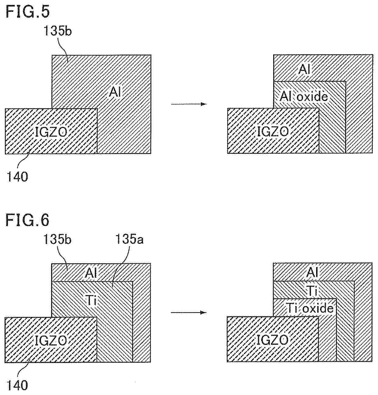
[0069]In the present invention, the reflective surface facing the backlight may be constituted by at least the source electrode layer 133 and the drain electrode layer 135. For example, the reflective surface may be constituted by the gate electrode layer 131, the source electrode layer 133, and the drain electrode layer 135. In Embodiment 3, the surface of each of the source electrode layer 133 and the drain electrode layer 135 on the transparent substrate 100 side (backlight side) is constituted by a high reflectance material such as Al. Thus, in the source electrode layer 133 and the drain electrode layer 135, the metal material contained in the portions connected to the semiconductor layer 140 is different from the metal material contained in the reflective surface.

[0070]FIG. 9 is an enlarged schematic plan view of one pixel of the TFT substrate of Embodiment 3. FIG. 10 is a schematic cross-sectional view illustrating the structure of the TFT substrate of Embodiment 3. Each soli...


PUM

PropertyMeasurementUnit
reflectanceaaaaaaaaaa
light reflectanceaaaaaaaaaa

Abstract

The present invention provides a liquid crystal display device including: a liquid crystal panel including a viewing surface side substrate, a liquid crystal layer, and a back surface side substrate; and a backlight including a reflector facing the back surface side substrate, wherein the liquid crystal panel in a plan view includes multiple pixel regions and a non-display region between the pixel regions, in the pixel regions, color filters are disposed, in the non-display region, a gate electrode layer, a source-drain electrode layer, and a semiconductor layer are disposed, the back surface side substrate includes a reflective surface facing the backlight in at least part of the non-display region, and the reflective surface is constituted by a metal material having a higher reflectance than a metal material contained in portions of the source-drain electrode layer that are connected to the semiconductor layer.

Description

CROSS-REFERENCE TO RELATED APPLICATIONS[0001]The present application claims priority under 35 U.S.C. § 119 to U.S. Provisional Patent Application No. 62 / 722,281 filed on Aug. 24, 2018, the contents of which are incorporated herein by reference in their entirety.BACKGROUND OF THE INVENTIONField of the Invention[0002]The present invention relates to liquid crystal display devices.Description of Related Art[0003]Liquid crystal display devices are display devices that utilize a liquid crystal composition to provide display. In their typical display system, a liquid crystal panel including a liquid crystal composition sealed between a pair of substrates is irradiated with light from a backlight. Voltage is applied to the liquid crystal composition to change the alignment of liquid crystal molecules, whereby the amount of light transmitted through the liquid crystal panel is controlled. Such liquid crystal display devices have features such as thin profile, light weight, and low power con...

Claims


Application Information

Patent Timeline
Patent Type & Authority Applications(United States)
IPC IPC(8): G02F1/1335H01L51/05
CPCH01L51/0525G02F1/133605G02F1/1333G02F1/133514G02F1/1343G02F1/13362G02F1/136209G02F2203/02H10K10/472
Inventor HIRAI, AKIRAMINOURA, KIYOSHIHASEBA, YASUHIROSAKAI, AKIRA
Owner SHARP KK
Why Eureka
Try Eureka