Top emission microled display and bottom emission microled display and a method of forming the same

a micro-led display and micro-led technology, applied in the field of top emission micro-led display and bottom emission micro-led display, can solve the problems of significant influence, thermal mismatch, and complex flip chip technology, and achieve the effect of preventing interference, color mixing and non-uniform display problems

Inactive Publication Date: 2020-03-12
PRILIT OPTRONICS INC
View PDF12 Cites 3 Cited by
  • Summary
  • Abstract
  • Description
  • Claims
  • Application Information

AI Technical Summary

Benefits of technology

[0010]In view of the foregoing, it is an object of the embodiment of the present invention to provide structures and forming methods of a top

Problems solved by technology

However, microLED is made by flip chip technology, while TFT is made by complementary metal-oxide-semiconductor (CMOS) process which is more complex than flip chip technology.
These two distinct technologies may cause thermal mismatch.
A drive current of the microLED is small in gray display, which may be significantly affected by leakage current.
When the size or the resolution of the display panel increases, output loading and delay of the drive circuits incr

Method used


Image

  • Top emission microled display and bottom emission microled display and a method of forming the same
  • Top emission microled display and bottom emission microled display and a method of forming the same
  • Top emission microled display and bottom emission microled display and a method of forming the same

Examples


first embodiment

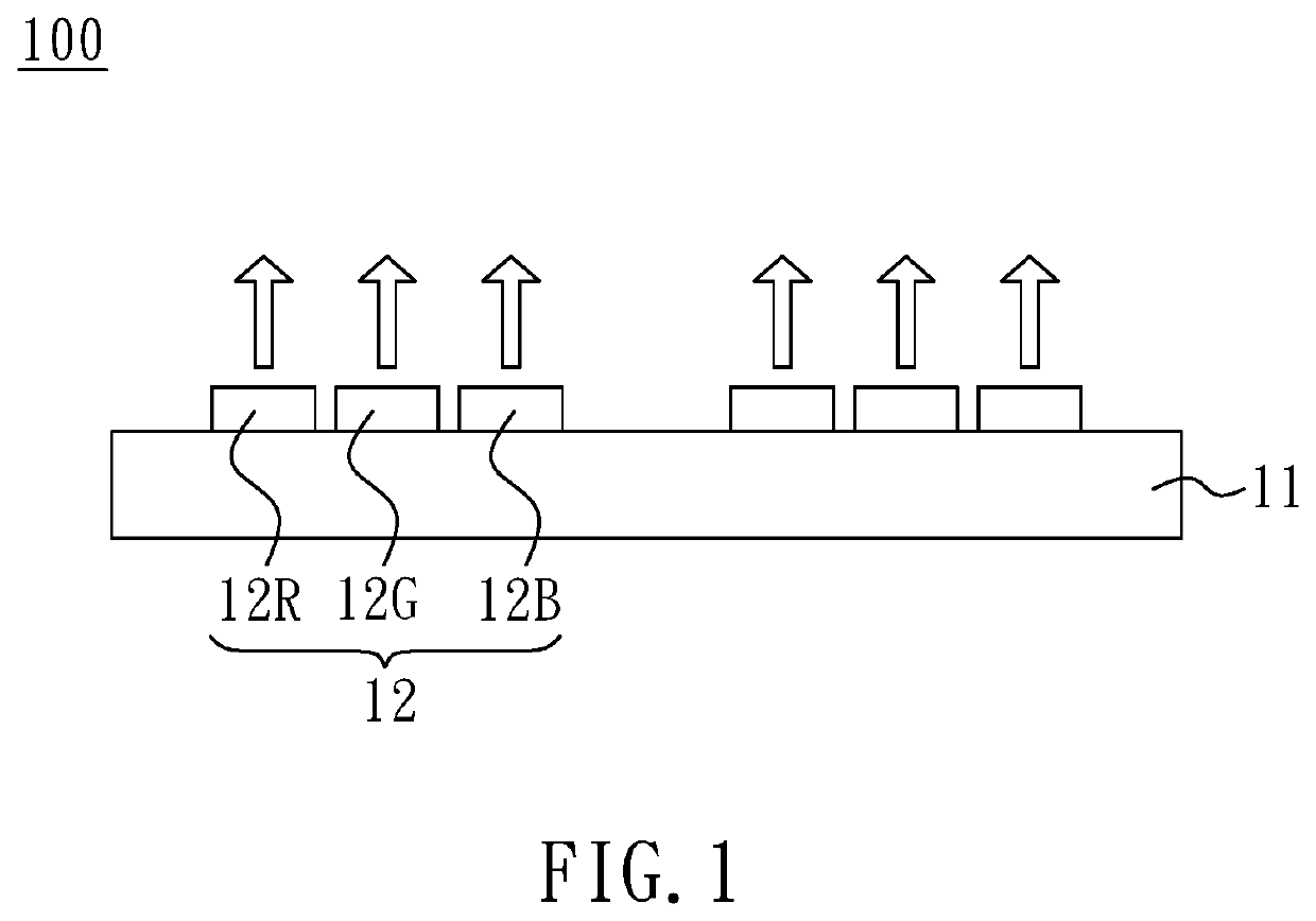
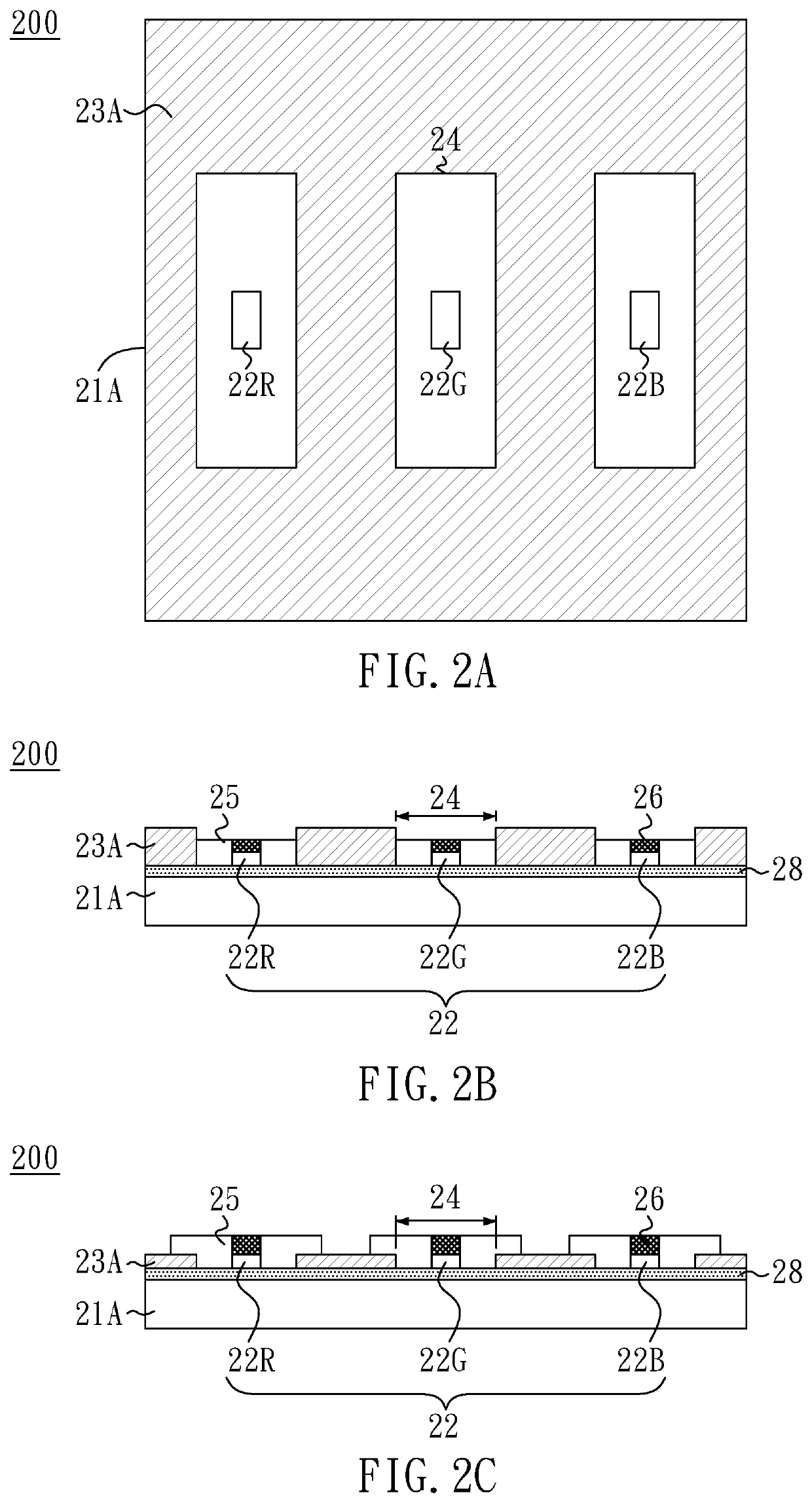
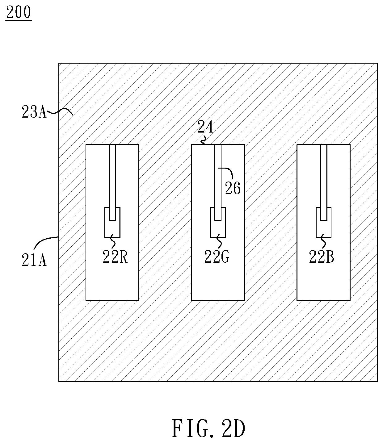
[0054]FIG. 2A shows a top view of a top emission microLED display 200 according to the present invention, and FIG. 2B shows a cross-sectional view of FIG. 2A. In the embodiment, microLEDs 22 (e.g., red microLED 22R, green microLED 22G and blue microLED 22B) may be disposed above a (first) main substrate 21A. A (first) light blocking layer 23A is disposed between adjacent microLEDs 22 and above the (first) main substrate 21A to prevent interference (e.g., color mixing) between adjacent microLEDs 22 and to enhance contrast. A bottom common electrode layer 28 may be disposed between the main substrate 21A and the microLEDs 22. In the present embodiment (and the following embodiments), the microLED 22 may be a rectangle, for example, with a length of 25 micrometers and a width of 10 micrometers. According to one aspect of the embodiment, the microLEDs 22 may be disposed longitudinally. That is, the length of the microLED 22 is parallel to the longitude of the display 200, and the width ...

second embodiment

[0063]FIG. 3C shows a cross-sectional view of a top emission microLED display 300 according to a modified second embodiment of the present invention. In the embodiment shown in FIG. 3C, the (first) light blocking layer 23A has a thickness less than the light guiding layer 25. Moreover, the (first) light blocking layer 23A and the light guiding layer 25 partially overlap each other, and the (first) light blocking layer 23A is partially covered with the light guiding layer 25.

[0064]FIG. 3D shows another top view of the top emission microLED display 300 according to the second embodiment of the present invention. A connecting structure 26, such as conductive electrode, is disposed on a top surface of the microLED 22 in each emission area 24. According to one aspect of the embodiment, the connecting structures 26 in the emission areas 24 have the same pattern and the connecting structures 26 in each emission area 24 have the same pattern, which can prevent nonuniform display issue.

third embodiment

[0065]FIG. 4A shows a top view of a top emission microLED display 400 according to the present invention, and FIG. 4B shows a cross-sectional view of FIG. 4A. In the embodiment, microLEDs 22 (e.g., red microLED 22R, green microLED 22G and blue microLED 22B) may be disposed above a (first) main substrate 21A. Each microLED 22 corresponds to an emission area 24. In the embodiment, a frame-shaped first light blocking layer 23A surrounds the emission area 24 and is disposed above the (first) main substrate 21A. In the embodiment, a blocking substrate 27 is disposed above the (first) main substrate 21A and the first light blocking layer 23A. A second light blocking layer 23B, which covers areas other than the emission areas 24 and the first light blocking layer 23A, is disposed on a bottom surface of the blocking substrate 27. The first light blocking layer 23A and the second light blocking layer 23B partially overlap each other. Accordingly, an aperture d1 of the first light blocking la...


PUM


Abstract

A microLED display includes a first main substrate, microLEDs disposed above the first main substrate, a first light blocking layer disposed above the first main substrate to define emission areas, a light guiding layer disposed in the emission areas, and a plurality of connecting structures disposed in the emission areas respectively and electrically connected with the microLEDs.

Description

CROSS-REFERENCE TO RELATED APPLICATIONS[0001]This application is a continuation application of U.S. application Ser. No. 16 / 128,255, filed on Sep. 11, 2018, the entire contents of which are herein expressly incorporated by reference.BACKGROUND OF THE INVENTION1. Field of the Invention[0002]The present invention generally relates to a light-emitting diode (LED) display, and more particularly to a top emission microLED display and a bottom emission microLED display.2. Description of Related Art[0003]A micro light-emitting diode (microLED, mLED or μLED) display panel is one type of flat display panel, which is composed of microscopic microLEDs each having a size of 1-10 micrometers.[0004]Compared to conventional liquid crystal display panels, the microLED display panels offer better contrast, response time and energy efficiency. Although both organic light-emitting diodes (OLEDs) and microLEDs possess good energy efficiency, the microLEDs, based on group III / V (e.g., GaN) LED technolog...

Claims


Application Information

Patent Timeline
IPC IPC(8): H01L27/15G03F7/00H01L33/36H01L33/62G09G3/20
CPCH01L33/36H01L33/62G09G3/2003G03F7/0007H01L27/156H01L25/0753H01L33/58G09G3/32
Inventor WU, BIING-SENGWU, CHAO-WEN
Owner PRILIT OPTRONICS INC
Why Eureka
Try Eureka