Liquid crystal panel and liquid crystal display device
a liquid crystal display and liquid crystal panel technology, applied in non-linear optics, identification means, instruments, etc., can solve the problems of line defect, defective product of liquid crystal panel, difficult to raise a yield, etc., and achieve suppressed the effect of the line defect and the reduction of the yield
- Summary
- Abstract
- Description
- Claims
- Application Information
AI Technical Summary
Benefits of technology
Problems solved by technology
Method used
Image

Examples
embodiment 1
[0042]Embodiment 1 according to the invention will be described below with reference to FIGS. 1 to 4.
(Configuration of Liquid Crystal Panel 1)
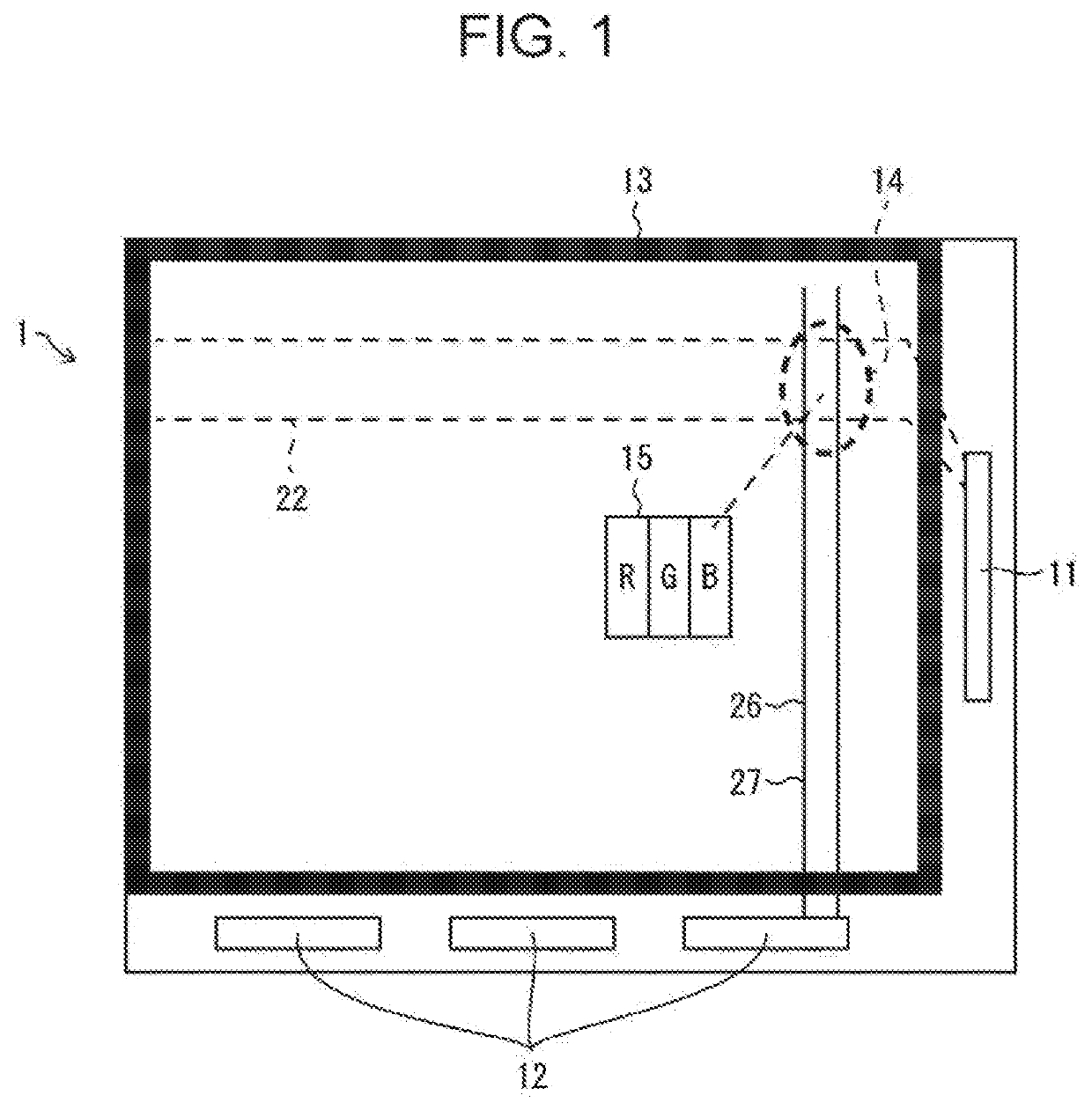
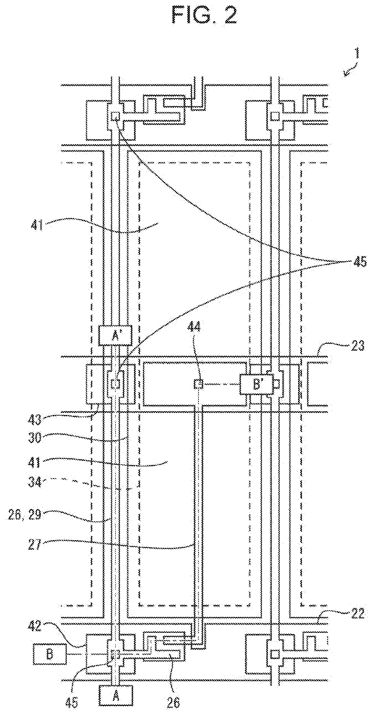
[0043]FIG. 1 is a block diagram illustrating a configuration of a main part of a liquid crystal panel 1 according to Embodiment 1 of the invention. As illustrated in the figure, the liquid crystal panel 1 includes a gate driver 11, a source driver 12, a plurality of gate lines 22 (first wires), a plurality of lower-layer source lines 26 (second wires, first source lines), and a plurality of upper-layer source lines 29 (third wires, second source lines). The gate lines 22 are arranged in a display region 13 so as to extend in a horizontal direction, and the respective lower-layer source lines 26 and the respective upper-layer source lines 29 are arranged in the display region 13 so as to extend in a vertical direction orthogonal to the gate lines 22. The upper-layer source lines 29 are arranged in parallel to the lower-layer source lines 26. In...
modified example
[0065]It is preferable that the contact hole 45 is arranged near a center of the gate line aperture 42 (or the auxiliary capacitance line aperture 43). It is thereby possible to effectively prevent a decrease in the pixel aperture ratio and a decrease in the display quality.
[0066]In the liquid crystal panel 1, the gate line aperture 42 is not necessarily required to be provided in all intersection portions in which the plurality of gate lines 22 and the plurality of lower-layer source lines 26 intersect. In other words, the gate line aperture 42 is only required to be provided in at least any of all of the intersection portions, and therefore the contact hole 45 is also only required to be provided in at least any of all of the intersection portions. For example, the contact hole 45 may not be provided in a part in which a columnar spacer by which a cell thickness of the liquid crystal panel 1 is maintained is installed. In this case, since an installation area of the columnar space...
embodiment 2
[0067]Embodiment 2 according to the invention will be described below with reference to FIGS. 13 to 15. In the present embodiment, a member that is common to Embodiment 1 is given the same member number, and detailed description thereof will not be repeated unless otherwise required.
(Configuration of Liquid Crystal Panel 1B)
[0068]FIG. 13 is a plan view planarly illustrating a liquid crystal panel 1B according to Embodiment 2 of the invention. The liquid crystal panel 1B includes respective members that are the same as respective members constituting the liquid crystal panel 1 according to Embodiment 1. However, the liquid crystal panel 1B and the liquid crystal panel 1 are different in a shape of the pixel electrode 30.
[0069]FIG. 14 is a plan view planarly illustrating the pixel electrode 30. As illustrated in the figure, the pixel electrode 30 has a so-called fish bone shape. The liquid crystal panel 1B operates in a VA (Vertical Alignment) mode. When a voltage is applied to the li...
PUM
| Property | Measurement | Unit |
|---|---|---|
| capacitance | aaaaa | aaaaa |
| insulating | aaaaa | aaaaa |
| flatness | aaaaa | aaaaa |
Abstract
Description
Claims
Application Information
 - R&D Engineer
- R&D Manager
- IP Professional
- Industry Leading Data Capabilities
- Powerful AI technology
- Patent DNA Extraction
Browse by: Latest US Patents, China's latest patents, Technical Efficacy Thesaurus, Application Domain, Technology Topic.
© 2024 PatSnap. All rights reserved.Legal|Privacy policy|Modern Slavery Act Transparency Statement|Sitemap