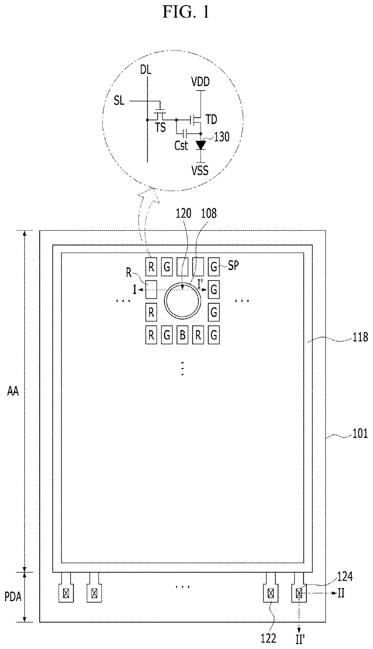
Display device

Active Publication Date: 2020-04-23
LG DISPLAY CO LTD
View PDF0 Cites 19 Cited by
  • Summary
  • Abstract
  • Description
  • Claims
  • Application Information

AI Technical Summary

Benefits of technology

The present patent provides a display device that reduces the non-display area, which is the space around the edges of the screen. This is achieved by using two through holes: one within the active area and one passing through the substrate. This design helps to minimize the bezel area and protect the light emitting stack from damage during the stripping process.

Problems solved by technology

For this reason, conventional display devices have a problem in that a display area is reduced.

Method used


Image

  • Display device
  • Display device
  • Display device

Examples


first embodiment

[0053]FIGS. 5A to 5E are cross-sectional views explaining a method for manufacturing an organic light emitting display device according to the present disclosure, that is, the organic light emitting display device illustrated in FIG. 2.

[0054]In detail, the multi-buffer layer and the active buffer layer included in the organic insulating layer 102 are formed on the substrate 101, as illustrated in FIG. 5A. Here, the substrate 101 is made of a plastic material having flexibility, to be bendable. For example, the substrate 101 is made of polyimide (PI), polyethylene terephthalate (PET), polyethylene naphthalate (PEN), polycarbonate (PC), polyethersulfone (PES), polyarylate (PAR), polysulfone (PSF), or cyclic-olefin copolymer (COC). The multi-buffer layer may be formed over the entirety of the substrate 101. The multi-buffer layer may provide an environment capable of more stably realizing thin film formation while enabling more effective execution of various processes before execution ...

second embodiment

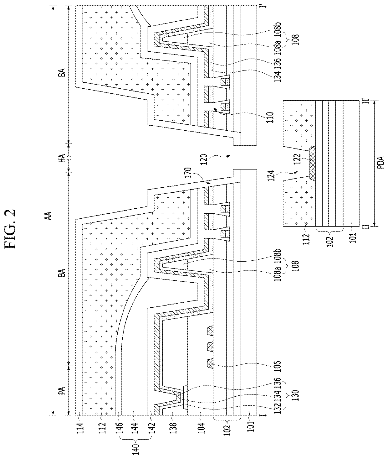
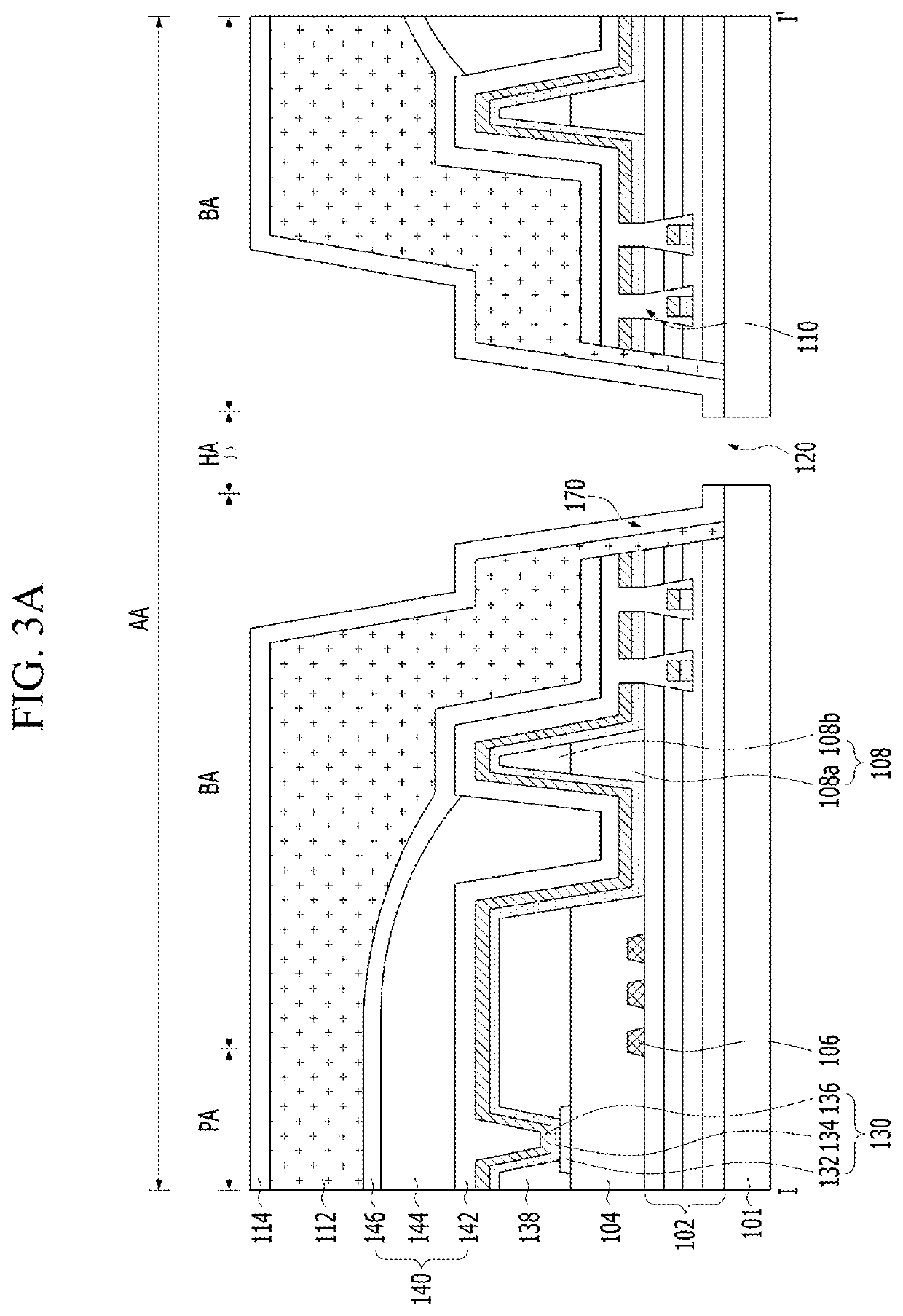
[0065]FIG. 6 is a cross-sectional view illustrating an organic light emitting display device according to the present disclosure.

[0066]The organic light emitting display device illustrated in FIG. 6 includes the same constituent elements as those of the organic light emitting display device illustrated in FIG. 2, except that a touch sensor is further included. Accordingly, no detailed description will be given of the same constituent elements.

[0067]The touch sensor includes a plurality of touch electrodes 152, and a plurality of bridges 154 connecting the touch electrodes 152.

[0068]The touch electrodes 152 may be constituted by a transparent conductive film made of ITO or IZO, may be constituted by a mesh metal film having a mesh structure, or may be constituted by a transparent conductive film as described above and a mesh metal film disposed over or beneath the transparent conductive film. Here, the mesh metal film is formed to have a mesh structure, using at least one conductive ...


PUM


Abstract

A display device capable of reducing a non-display area is disclosed. The disclosed display device includes a first through hole not overlapping with an organic cover layer surrounding at least one hole area disposed within an active area, and a second through hole passing through a substrate. Accordingly, it is possible to minimize a bezel area, which is a non-display area, and to prevent damage to a light emitting stack caused by a stripping process.

Description

CROSS-REFERENCE TO RELATED APPLICATION[0001]This application claims the benefit of Korean Patent Application No. 10-2018-0125211 filed on Oct. 19, 2018, which is hereby incorporated by reference as if fully set forth herein.BACKGROUNDTechnical Field[0002]The present disclosure relates to a display device, and more particularly to a display device capable of reducing a non-display area.Description of the Related Art[0003]An image display device, which renders a variety of information on a screen, is a core technology of the information age. Such an image display device is developing towards enhanced thinness, enhanced lightness, and enhanced portability as well as enhanced performance. In connection with this, a slim display device capable of eliminating disadvantages of heavy and bulky structures of cathode ray tubes (CRTs) is highlighted.[0004]Representative examples of such a slim display device may include a liquid crystal display (LCD) device, a plasma display panel (PDP), an or...

Claims


Application Information

Patent Timeline
IPC IPC(8): H01L51/52H01L27/32
CPCH01L27/3258H01L51/5253H01L27/323H01L27/3234H10K59/122H10K59/123H10K59/124H10K59/1213H10K65/00H10K59/65H10K59/873H10K59/40H10K59/82H10K50/844
Inventor YUN, JEONG-GINAM, KYOUNG-JINLEE, YOUNG-WOOKPARK, JONG-HAN
Owner LG DISPLAY CO LTD
Why Eureka
Try Eureka