Light emitting package structure and method of manufacturing the same

a technology of light-emitting packages and packaging materials, which is applied in the direction of basic electric elements, electrical appliances, semiconductor devices, etc., can solve the problems of reducing the yield of mounting technology, affecting the quality of light-emitting packages, so as to reduce the loss of rejected materials and reduce customer complaints.

Inactive Publication Date: 2020-06-04
LITE ON OPTO TECH (CHANGZHOU) CO LTD +1
View PDF4 Cites 1 Cited by
  • Summary
  • Abstract
  • Description
  • Claims
  • Application Information

AI Technical Summary

Benefits of technology

[0007]In response to the above-referenced technical inadequacies, the present disclosure provides a light emitting package structure and a method of manufacturing the same, so as to improve on issues relating to poor mounting yield due to CSP surface adhesion, reduce the loss of rejected materials, and reduce customer complaints.
[0010]One of the beneficial effects of the present disclosure is that with the technical solution of “the encapsulant having an anti-adhesion upper surface and an anti-adhesion surrounding surface,” the light emitting package structure and the method of manufacturing the same provided by the present disclosure can reduce the surface adhesion of the light emitting package structure and improve the mounting yield.

Problems solved by technology

However, since the silicone material is viscous and easily adheres to a carrier tape, the yield from mounting technology is decreased.
Specifically, the structure of the CSP merely includes a light emitting chip having five sides covered by silicone, so that the adhesion issue of the silicone material occurs often in the CSP.
However, the silicone thus treated often ends up with uneven coating, without coating on the sides, and having higher hardness, so as to be easily broken or have poor reliability.

Method used


Image

  • Light emitting package structure and method of manufacturing the same
  • Light emitting package structure and method of manufacturing the same
  • Light emitting package structure and method of manufacturing the same

Examples


embodiment 1

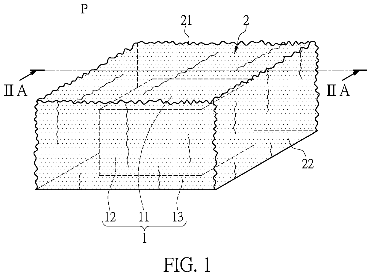
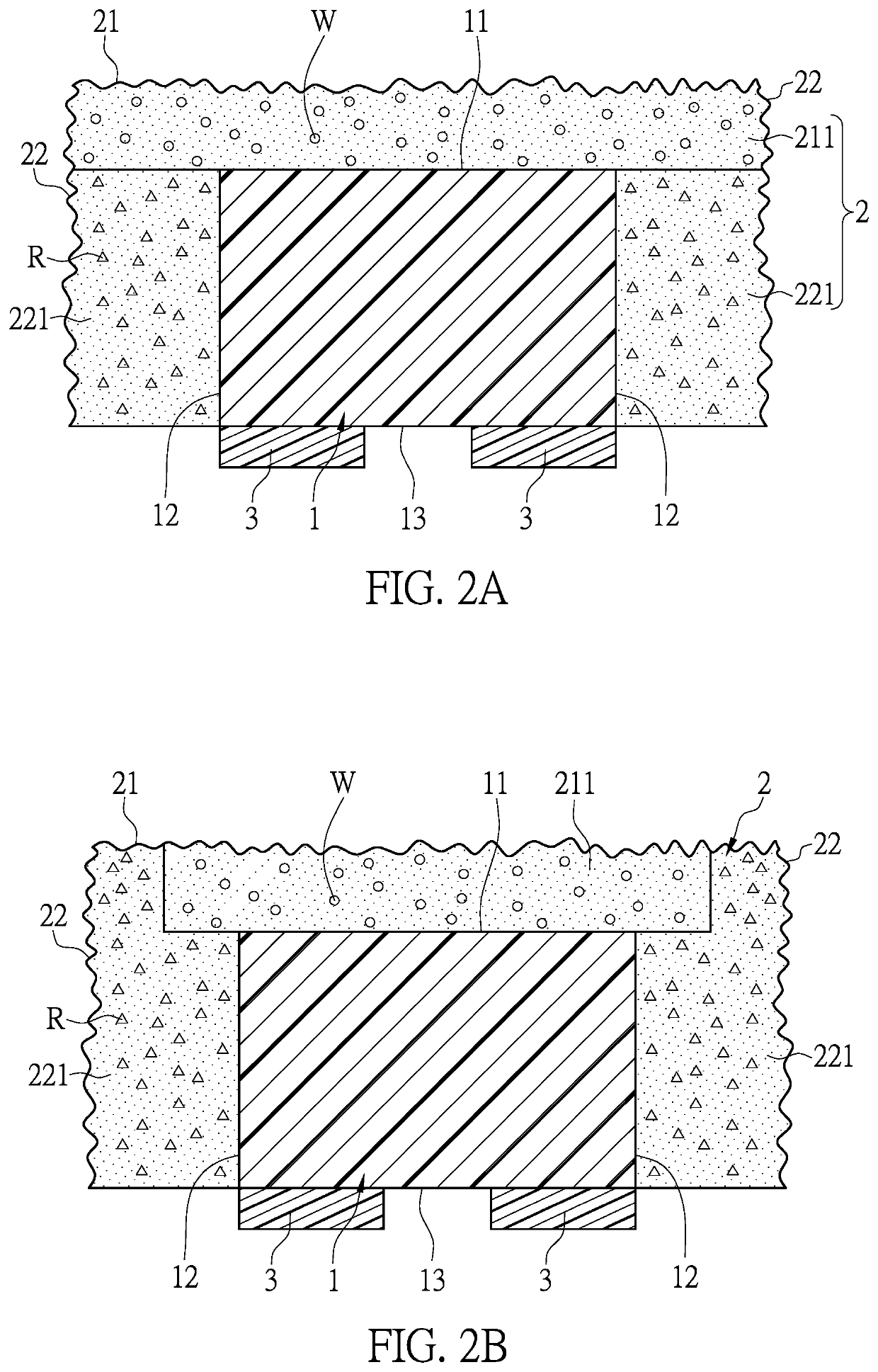
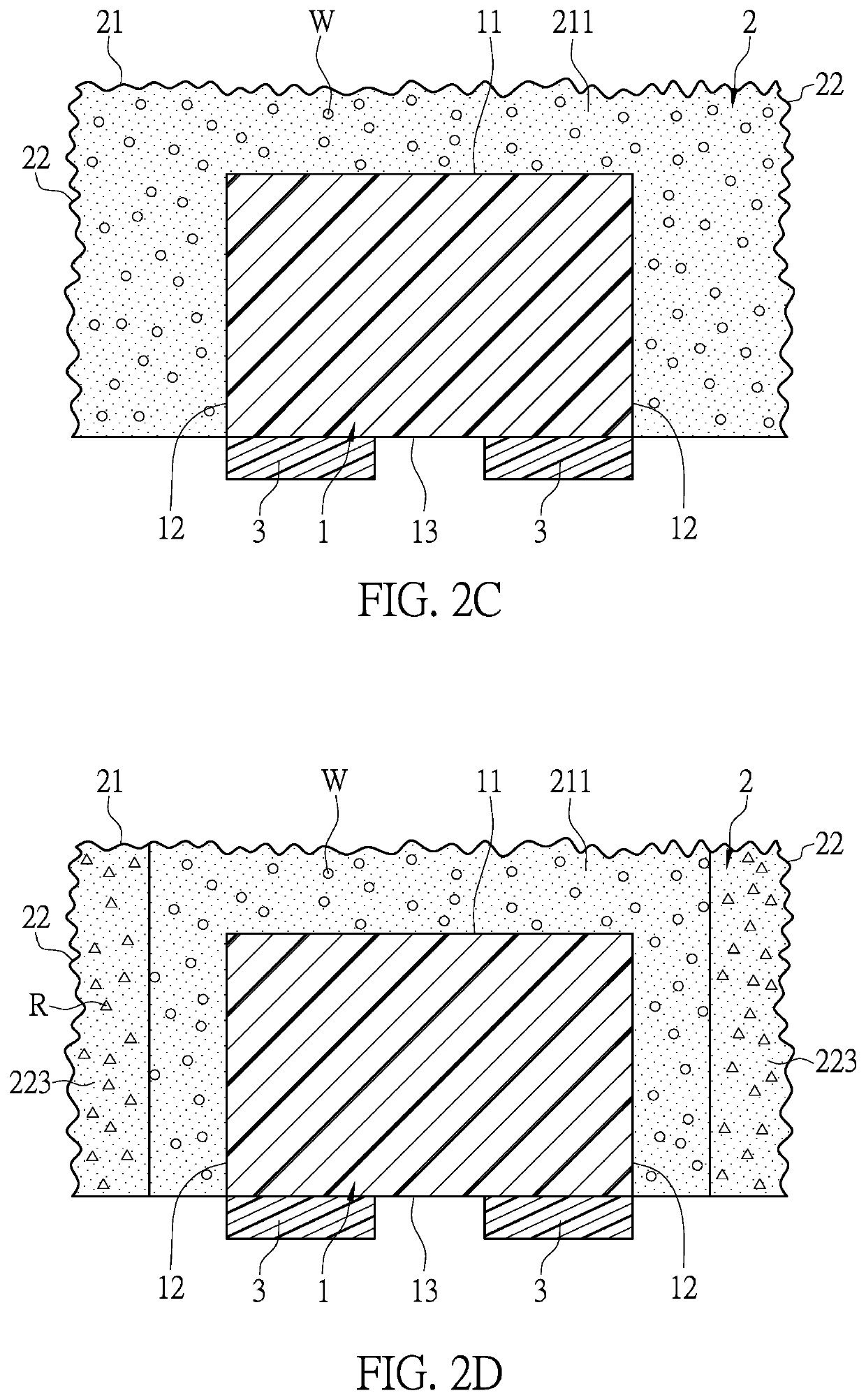
[0051]Firstly, the plurality of light emitting chips are arranged and configured on the temporary carrier, and the silicone is mixed with the wavelength conversion material to serve as the encapsulant and to be disposed on the light emitting chip and the temporary carrier. At this time, the encapsulant is filled into the gaps between the plurality of light emitting chips, and the light transmissive layer is formed on the plurality of light emitting chips. A cutting tool is used to cut the encapsulant along a predetermined cutting path to obtain the plurality of independent light emitting package structures having the light emitting chip and the light transmissive layer. Then, argon (Ar) plasma is used to treat the surface of the light transmissive layer of the light emitting package structure at a frequency of 400 W for 12 minutes. Finally, the temporary carrier is removed.

embodiment 2

[0052]Firstly, the plurality of light emitting chips are arranged and configured on the temporary carrier, and the silicone mixed with the reflective material is disposed on the temporary carrier without covering the light emergent surfaces of the light emitting chips. The reflection layer is filled into the gaps between the plurality of light emitting chips. The silicone mixed with the wavelength conversion material is disposed on the reflection layer and the light emergent surfaces of the light emitting chips to form the light transmissive layer.

[0053]A cutting tool is used to cut the encapsulant along a predetermined cutting path to obtain the plurality of independent light emitting package structures having the light emitting chip, the reflection layer and the light transmissive layer. Then, a grinding machine is used to surface treat the surface of the light emitting package structure by grinding with alumina powders for 30 minutes. Finally, the temporary carrier is removed.

[00...


PUM

PropertyMeasurementUnit
anti-adhesionaaaaaaaaaa
roughness ratioaaaaaaaaaa
wavelengthaaaaaaaaaa

Abstract

A light emitting package structure includes: a light emitting chip, an encapsulant covering the light emitting chip and having an anti-adhesion upper surface and an anti-adhesion surrounding surface. A method of manufacturing a light emitting package structure is further provided and includes: configuring a plurality of light emitting chips on a temporary carrier; forming an encapsulant to cover the plurality of light emitting chips; cutting the encapsulant to form the independent light emitting package structure; and surface treating the cut encapsulant such that the encapsulant has an anti-adhesion upper surface and an anti-adhesion surrounding surface.

Description

CROSS-REFERENCE TO RELATED PATENT APPLICATION[0001]This application claims the benefit of priority to China Patent Application No. 201811453487.3, filed on Nov. 30, 2018 in People's Republic of China. The entire content of the above identified application is incorporated herein by reference.[0002]Some references, which may include patents, patent applications and various publications, may be cited and discussed in the description of this disclosure. The citation and / or discussion of such references is provided merely to clarify the description of the present disclosure and is not an admission that any such reference is “prior art” to the disclosure described herein. All references cited and discussed in this specification are incorporated herein by reference in their entireties and to the same extent as if each reference was individually incorporated by reference.FIELD OF THE DISCLOSURE[0003]The present disclosure relates to a light emitting package structure and a method of manufac...

Claims


Application Information

Patent Timeline
Patent Type & Authority Applications(United States)
IPC IPC(8): H01L33/52H01L33/50H01L33/46
CPCH01L33/502H01L33/52H01L33/46H01L33/54H01L33/10H01L33/005H01L33/50H01L2933/0091H01L33/56H01L33/60
Inventor CHEN, CHIH-YUANLEE, TIEN-YUHUANG, CHIEN-TUNGTSAI, WEI-LUN
Owner LITE ON OPTO TECH (CHANGZHOU) CO LTD
Why Eureka
Try Eureka