

Light emitting unit
- Summary
- Abstract
- Description
- Claims
- Application Information
AI Technical Summary
Benefits of technology
Problems solved by technology
Method used
Image

Examples
first embodiment
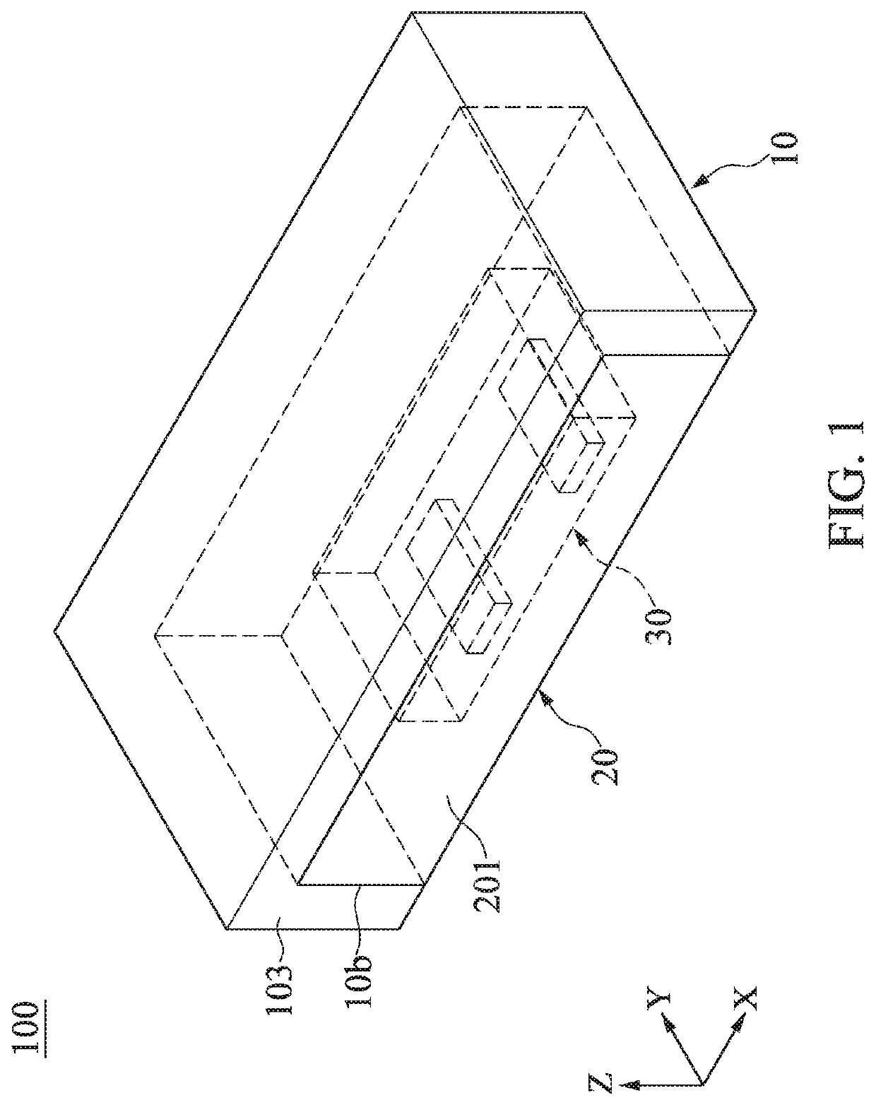
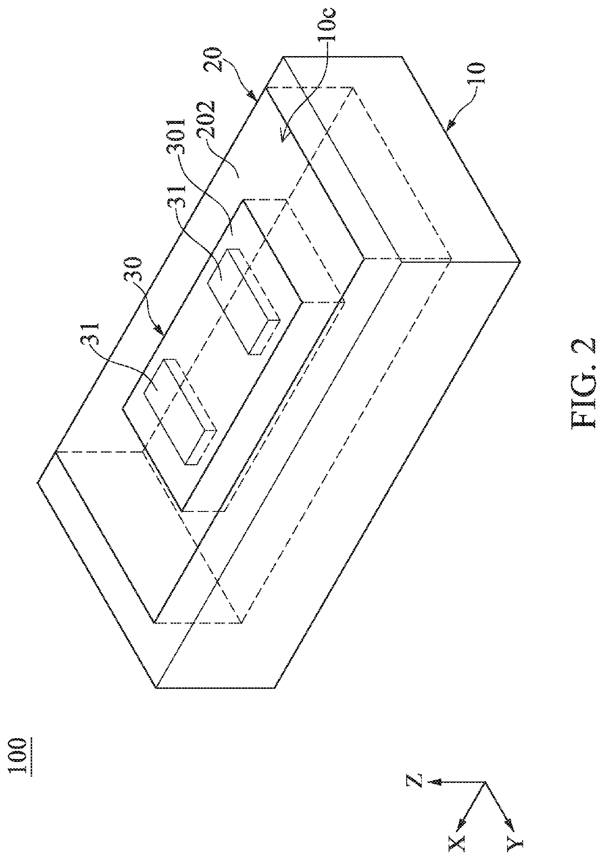
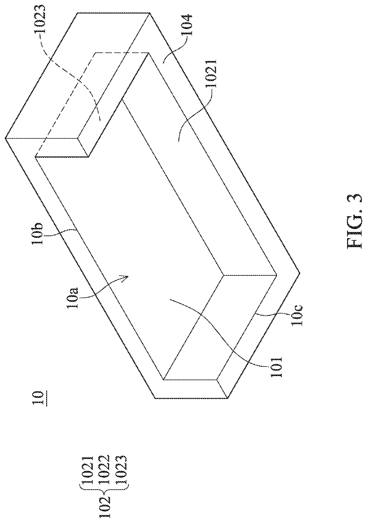
[0042]FIG. 1 to FIG. 5 show a light emitting unit according to the present disclosure. FIG. 1 is a schematic view of the light emitting unit of the present disclosure, FIG. 2 is a schematic view of the light emitting unit of the present disclosure from another angle of view, FIG. 3 is a schematic view of a reflective structure of the light emitting unit of the present disclosure, FIG. 4 is a cross sectional view of the light emitting unit of the present disclosure, and FIG. 5 is a front view of the light emitting unit of the present disclosure.
[0043]A light emitting unit 100 includes a reflective structure 10, a light transmitting body 20 and a light emitting chip 30. The reflective structure 10 covers the light transmitting body 20 and the light transmitting body 20 covers the light emitting chip 30.
[0044]In FIG. 3, two outer side surfaces of the reflective structure 10 are adjacent to each other and respectively include a side opening 10b and a bottom opening 10c. The reflective s...
second embodiment
[0058]FIG. 6 toFIG. 9 are schematic views of the light-emitting unit according to the present disclosure. The main difference between this embodiment and the foregoing embodiment lies in that: a cross-section width of the recess 10a extends toward the side opening 10b. Namely, the cross-section width of the recess 10a will be larger when being closer to the side opening 10b, such that the luminous efficacy of the entire light emitting unit can be improved. In other words, the recess 10a is roughly a trapezoidal cube.
[0059]Specifically, in this embodiment, the electrode exposing surface 202 of the light transmitting body 20 can be a trapezoidal surface having an upper base 2021, a lower base 2022 and two legs 2023. The upper base 2021 is disposed away from the light emitting surface 201, the lower base 2022 is disposed adjacent to the light emitting surface 201, and a width D1 of the upper base 2021 in a lateral direction (the X-axis direction shown in the drawings) is smaller than a...
third embodiment
[0066]FIG. 10 is a side cross sectional view of the light-emitting unit according to the present disclosure. The main difference between this embodiment and the foregoing embodiments lies in that: an included angle θ6 between the first section surface 1021 and the electrode exposing surface 202 can be greater than 90 degrees. That is, an included angle θ7 is formed between the first section surface 1021 and a vertical line (the Y-axis in the figure). In practical applications, the included angle θ7 formed by the first section surface 1021 and the vertical line is less than 5 degrees. Based on the above, in this embodiment the light beam emitted by the fourth light emitting surface 3034 is more easily to be reflected by the first section surface 1021 and emits toward the light emitting surface 201, thereby improving the use of the light beam emitted by the light emitting chip 30.
[0067]It should be noted that referring to FIG. 2, FIG. 7 and FIG. 9, in practical applications, the amoun...
PUM
 Abstract
Description
Claims
Application Information