Transparent conductive film, method of producing the same, flexible organic electronic device, and organic thin-film solar battery
Inactive Publication Date: 2014-07-03
FUJIFILM CORP
View PDF6 Cites 8 Cited by
Summary
Abstract
Description
Claims
Application Information
AI Technical Summary
This helps you quickly interpret patents by identifying the three key elements:
Problems solved by technology
Method used
Benefits of technology
Benefits of technology
The invention is a transparent conductive film that can be used in various applications such as organic thin-film solar batteries and organic EL devices. The film has a structure that allows it to function as a positive electrode or negative electrode, depending on the device. The film has a plastic support that is transparent to light in the wavelength range from400 nm to800 nm, which can hold a conductive stripe, bus lines, and other components of the device. The support can be made of various resins like polyester, methacryl resin, polyimide, etc. The film can be produced by coating a conductive material onto a plastic support and patterning it to create the desired electrodes. The technical effects of the invention include improved stability, durability, and flexibility of the conductive film, as well as improved performance and reliability of devices that use it.
Problems solved by technology
However, they are not suitable for a roll-to-roll production process, and they cannot sufficiently achieve the purpose of providing an inexpensive transparent conductive film.
This is a problem with applying the silver ink to polyethylene terephthalate (PET), which is an inexpensive plastic substrate.
Method used
Image
Click on the blue label to locate the original text in one second.
Reading with bidirectional positioning of images and text.
Examples
examples
[0145]Hereinafter, the present invention is more specifically described using examples. The materials, amounts of the materials used, ratios, contents of treatments, procedures, etc., shown in the following examples can be modified as appropriate without departing from the spirit of the invention. Therefore, the scope of the invention is not limited to the specific examples shown below.
example 1-2
Formation of Conductive Stripe
[0151]A copper stripe film was produced in the same manner as in Example 1 (the transparent conductive film F-1), except that the metal material forming the conductive stripe was changed from silver to copper.
[0152]On the surface of the thus formed film, an aqueous dispersion of polyethylenedioxythiophene / polystyrenesulfonate (abbreviated as PEDOT-PSS) (ORGACON S-305, available from Agfa) was spin-coated. Then, this film was dried by heating at 110° C. for 20 minutes to form a conductive polymer layer. The thickness of the conductive polymer layer was 100 nm.
[0153]In this manner, a transparent conductive film (F-6) of Example 1-2 shown in Table 1 was obtained.
[0154]Separately from this, the conductive polymer layer was formed in the same manner as described above on a 25 mm×25 mm PET film without the conductive stripe vapor-deposited thereon, and the surface resistance value was found to be 220Ω / □. Based on this res...
examples 4 to 6
Production of Transparent Conductive Film
[0165]Transparent conductive films (F-11 to F-13) were produced in the same manner as the production of the transparent conductive film (F-1) of Example 1, except that the mask was slid during the vapor deposition of silver. The holder of the mask was movable, and the sliding was achieved using a stepper motor for a vacuum chamber. The sliding direction was perpendicular to the stripe in the plane of the mask. The sliding width was 0.05 mm. The film thickness and the line width of the formed conductive stripe was as shown in Table 2. The line width was increased by the sliding width, and the cross-section of the stripe in the perpendicular direction had an isosceles trapezoidal shape where the thickness decreased toward each end.
[0166]Using the transparent conductive films (F-11 to F-13), organic thin-film solar batteries (P-11 to P-13) of Examples 4 to 6 were produced in the same manner as in Exam...
PUM
Property
Measurement
Unit
Length
aaaaa
aaaaa
Length
aaaaa
aaaaa
Length
aaaaa
aaaaa
Abstract
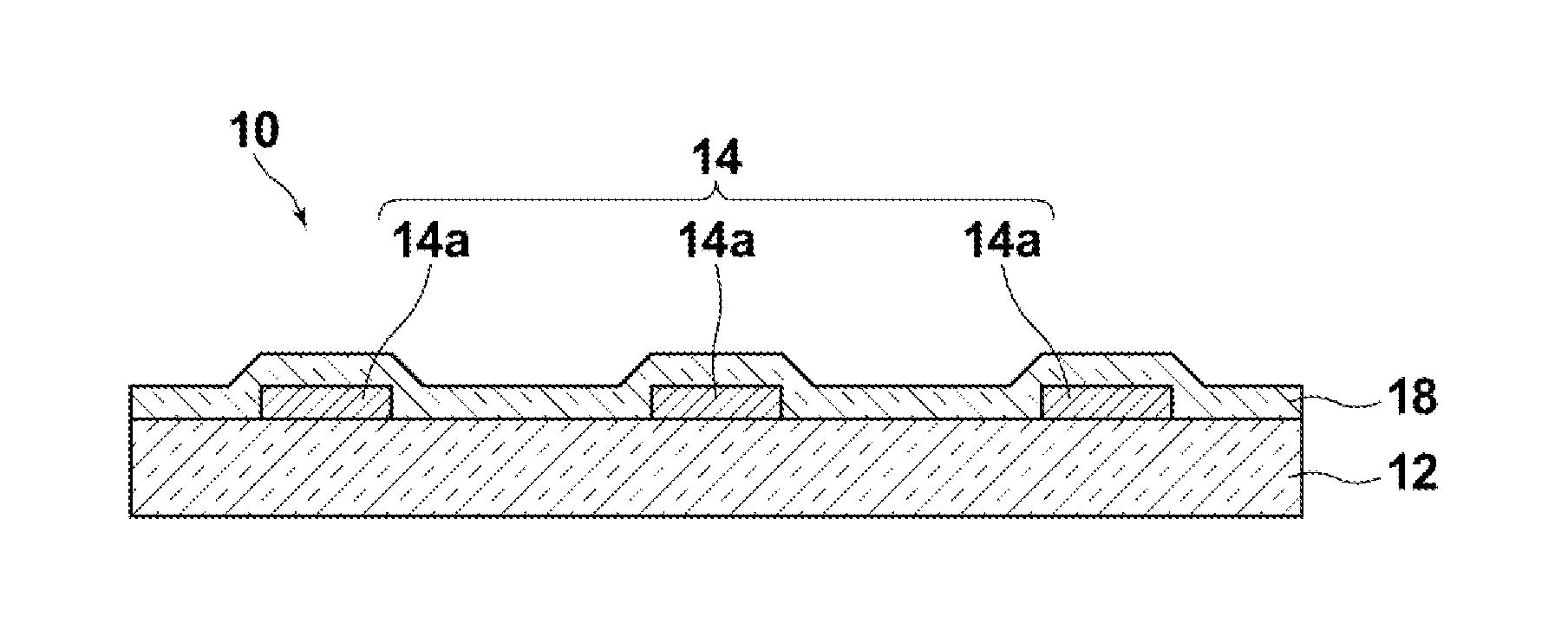
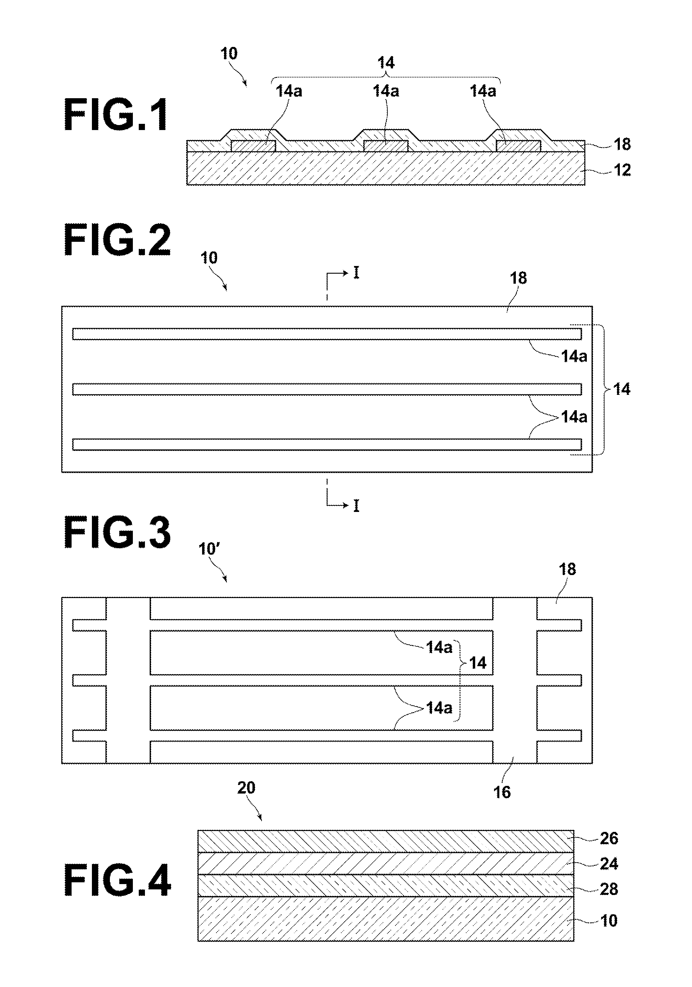
A transparent conductive film includes: a conductive stripe formed on a plastic support by a maskdeposition process, the conductive stripe including a plurality of conductive lines made of a metal or an alloy having a film thickness of not less than 50 nm and not greater than 500 nm and a line width of not less than 0.3 mm and not greater than 1 mm in plan view and being arranged at an interval of not less than 3 mm and not greater than 20 mm; and a transparent conductive material layer formed to cover the plastic support and the conductive stripe, the transparent conductive material having a specific resistance of not greater than 4×10⁻³ Ω·cm and a film thickness of not less than 20 ma and not greater than 500 nm.
Description
TECHNICAL FIELD[0001]The present invention relates to a transparent conductive film and a simple production method thereof, as well as an organic thin-film electronic device and an organic thin-film solar battery using the transparent conductive film.BACKGROUND ART[0002]In recent years, flexible electronic devices as soft matters are attracting attention. In particular, there are higher and higher expectations for flexible organic electronic devices that are expected to achieve lightweight and low production cost, specifically, organic thin-film solar batteries and flexible organic EL devices (or organic electroluminescence devices).[0003]A typical structure of flexible organic electronic devices includes an electron-conductive organic thin film and / or a hole-conductive organic thin film disposed between two dissimilar electrodes, at least one of which is transparent. Such flexible organic electronic devices have an advantage that the production thereof is easier than production of ...
Claims
Application Information
Patent Timeline
Application Date:The date an application was filed.
Publication Date:The date a patent or application was officially published.
First Publication Date:The earliest publication date of a patent with the same application number.
Issue Date:Publication date of the patent grant document.
PCT Entry Date:The Entry date of PCT National Phase.
Estimated Expiry Date:The statutory expiry date of a patent right according to the Patent Law, and it is the longest term of protection that the patent right can achieve without the termination of the patent right due to other reasons(Term extension factor has been taken into account ).
Invalid Date:Actual expiry date is based on effective date or publication date of legal transaction data of invalid patent.

