
Device for Attaching Two Elements Such as a Chip, an Interposer and a Support

a technology of two elements and supporting, which is applied in the field of devices for attaching two elements in the microelectronics, can solve the problems of increasing the bulk of the mounting device between the chip and the supporting, and not allowing the chip to be correctly attached to the supporting, so as to improve the dissipation of stresses and improve the holding and adhesion of the attachment area

Inactive Publication Date: 2020-06-25
TRONICS MICROSYST
View PDF73 Cites 0 Cited by
  • Summary
  • Abstract
  • Description
  • Claims
  • Application Information

AI Technical Summary

Benefits of technology

The disclosed embodiments allow for precise adjustment of the attachment layer between two elements, which results in reduced mechanical stress between them. This is achieved by eliminating the need for an interposer in the process.

Problems solved by technology

This is more particularly the case for micro-manufactured chips the fine and sensitive mechanical structures thereof having, once assembled, localized or extended stress points that may disrupt the operation of the product.
However, this solution, by using both an interposer and columns, greatly increases the bulk of the mounting device between the chip and the support.
However, insofar as the surface of the stud in contact with the support is often insufficient, this solution does not allow the chip to be correctly attached to the support.
The technical problem of the therefore consists in limiting the attachment surface between a chip and a support or an interposer while guaranteeing the quality of the attachment, while separating the attachment areas from the sensitive areas of the chip.

Method used


Image

  • Device for Attaching Two Elements Such as a Chip, an Interposer and a Support
  • Device for Attaching Two Elements Such as a Chip, an Interposer and a Support
  • Device for Attaching Two Elements Such as a Chip, an Interposer and a Support

Examples


Embodiment Construction

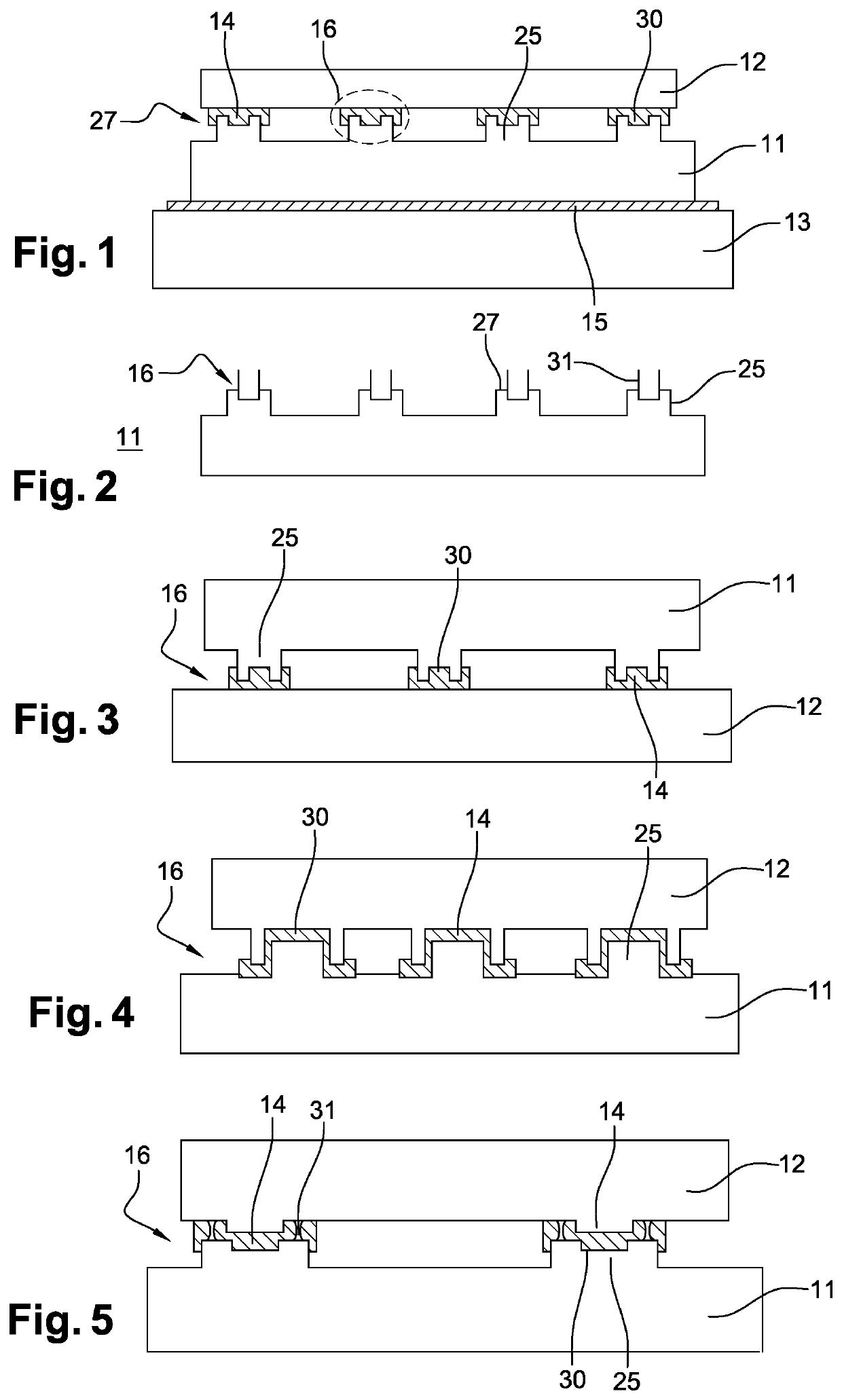
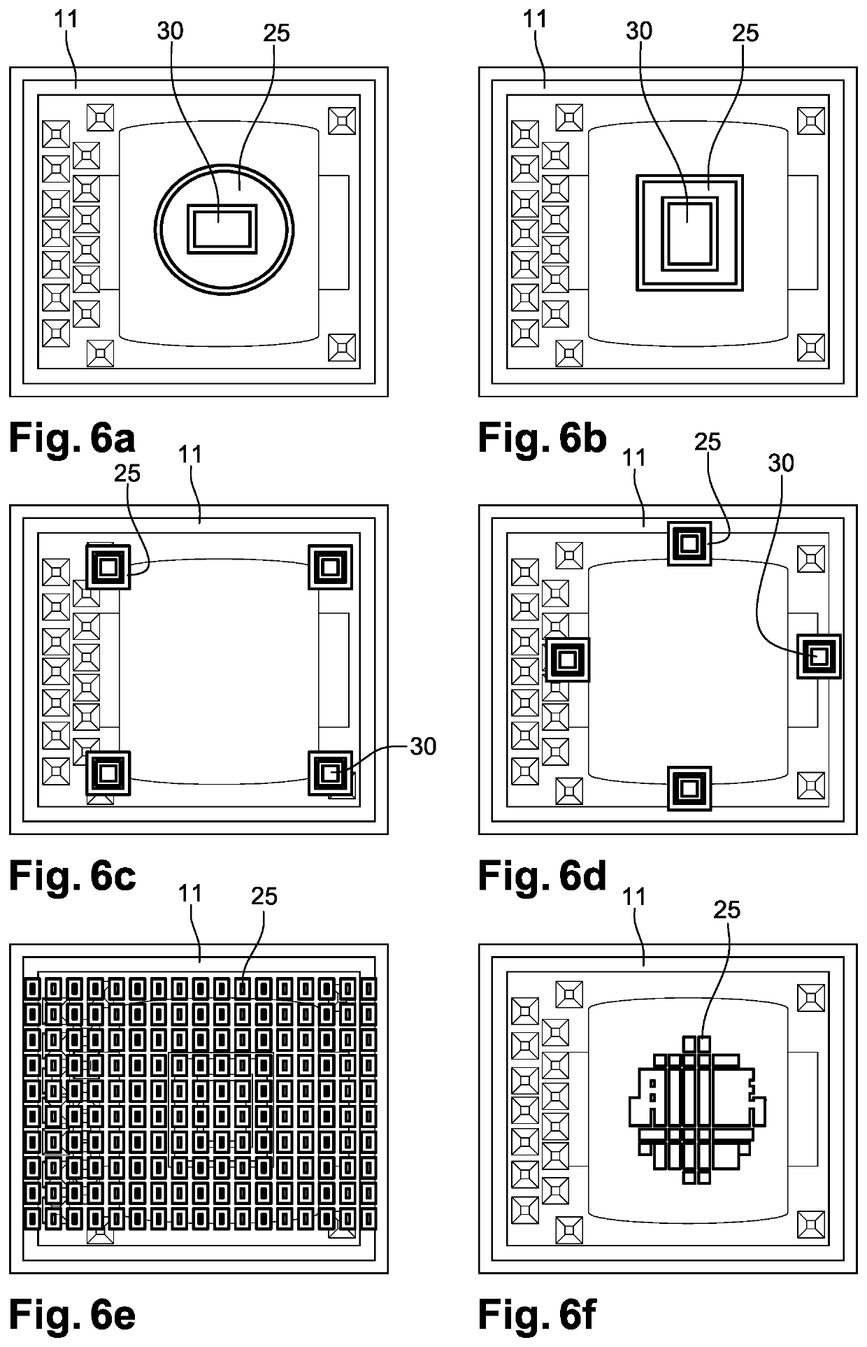
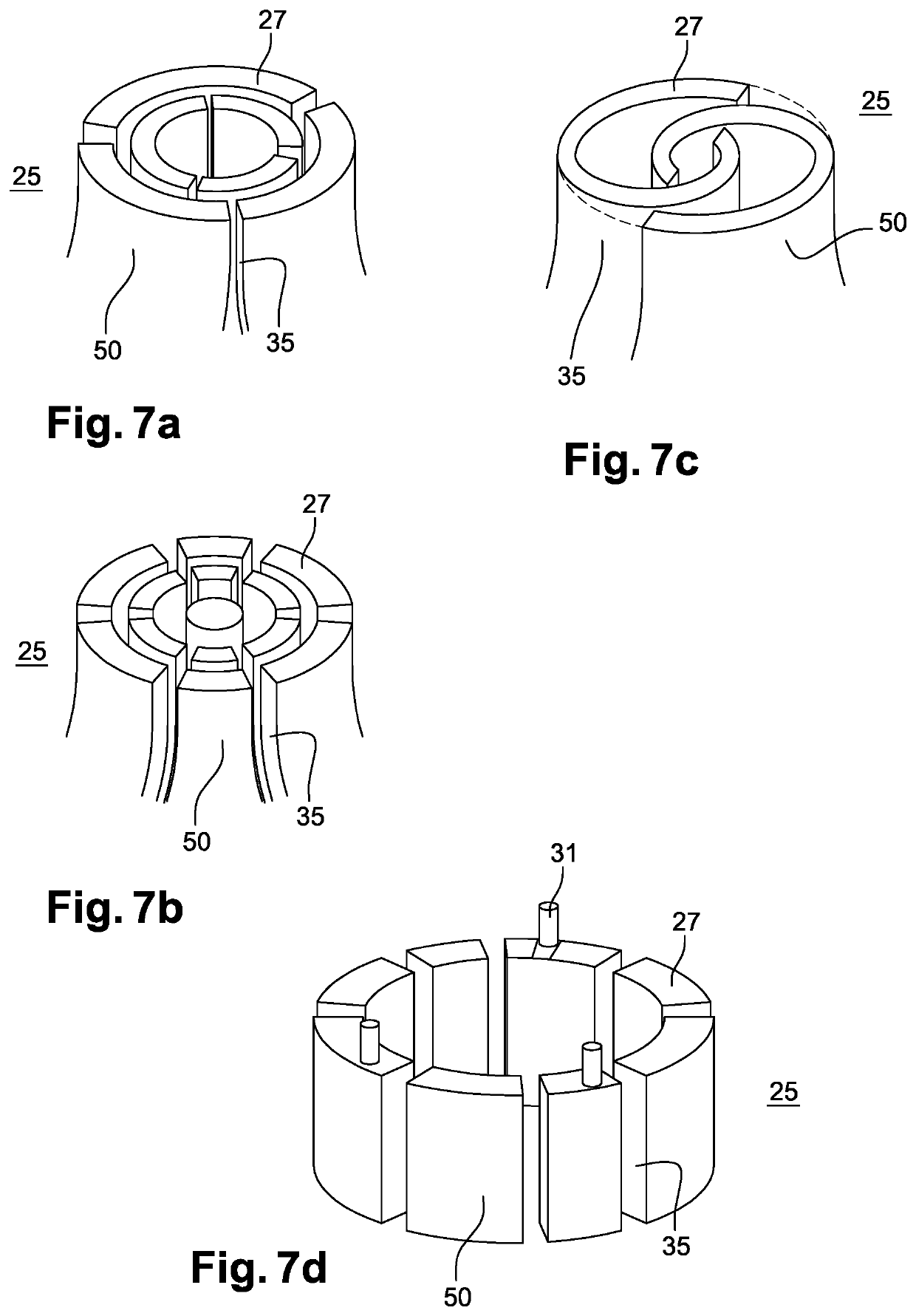
[0034]The disclosed embodiments make it possible to connect a chip and a support directly or by means of an interposer. When there is no interposer, the embodiments are implemented between the chip and the support. When there is an interposer, the embodiments can be implemented between the chip and the interposer, between the interposer and the support or both. To cover all of these embodiments, the description describes two elements 11, 12 between which the described embodiments are implemented. These elements 11, 12 are a chip, an interposer or a support. Amongst these elements 11, 12, the first element 11 is distinguished as being that which bears at least one stud 25.

[0035]FIG. 1 illustrates a chip connected to a support by means of an interposer. The contemplated embodiments are implemented between two elements 11, 12, which are the chip and the interposer. The support then corresponds to a third element 13. A first element 11, the interposer, includes a lower face connected to...


PUM


Abstract

A device for attaching two elements such as a chip, an interposer and a support, at least one of said two elements being micro-manufactured. The device includes at least one projecting stud structured in a first element extending facing the second element, the stud being configured to create an attachment area between one end of the stud and the second element. The device also includes an attachment layer deposited in the attachment area so as to attach the stud to the second element, and a recess made in the attachment area such that the attachment layer extends at least partially into the recess.

Description

TECHNICAL FIELD[0001]The present disclosure concerns a device for attaching two elements in the microelectronics field such as a chip, an interposer and a support, at least one of said two elements being micro-manufactured. The disclosed embodiments make it possible to attach a micro-manufactured chip onto a support with or without an interposer. The disclosed embodiments are particularly advantageously applicable to sensors of the accelerometer or gyrometer type, pressure sensors, optical components or power components.BACKGROUND[0002]Micro-manufactured chips comprise chips that are highly sensitive to external conditions, such as MEMS (micro-electromechanical system) chips or MOEMS (micro-opto-electromechanical system) chips. Micro-manufactured chips are sometimes sensitivity to thermomechanical stresses experienced by the support upon which the chip is mounted due to the difference in the thermal expansion coefficient between the silicon chip (TEC comprised between 2 and 4 ppm / ° ...

Claims


Application Information

Patent Timeline
Patent Type & Authority Applications(United States)
IPC IPC(8): B81B7/00H01L23/00
CPCH01L2224/32148H01L2924/1461B81B7/0048H01L24/32H01L2924/351H01L2224/32147
Inventor VOLANT, VALÉRIEGIGAN, OLIVIERLECLERC, JACQUES
Owner TRONICS MICROSYST
Learn More