
3D NAND - high aspect ratio strings and channels

a high aspect ratio, string and channel technology, applied in the field of nonvolatile storage, can solve the problems of increasing the chance of defects within the layers, adversely affecting the compounded yield, and difficulty in forming channels and slits using typical etching through 64 or more layers of silicon oxide and silicon nitride, and reducing the efficiency of etching.

Active Publication Date: 2020-06-25
XCELSIS CORP
View PDF4 Cites 1 Cited by
  • Summary
  • Abstract
  • Description
  • Claims
  • Application Information

AI Technical Summary

Benefits of technology

The patent text describes methods for forming a memory cell stack in 3D NAND memory. The methods involve forming layers on a substrate, etching holes in the layers, and depositing additional layers on top of the layers. The holes can be filled with conductive material or dielectric material, and the layers can be bonded together. The technical effects of the patent text include improved memory cell density and more efficient memory cell formation.

Problems solved by technology

In this regard, as the number of layers in the stack increases, such as to more than 64, the chance for defects within the layers increases, as the defect may propagate through the stack and compounded yield may be adversely affected.
However, forming the channels and slits using typical etching through a large stack of silicon oxide and silicon nitride layers, such as 64 or more layers, is difficult and time consuming with current etching technologies.
In this regard, a trillion or more holes may be required on a single substrate and consistently forming these holes may be difficult at such a small scale.
Such defects can lead to shorts, interference between neighboring memory strings, and other performance issues affecting the product yield
Filling the holes formed by etching with conformal layers of silicon oxide, silicon nitride, silicon oxynitride, and polysilicon to form the memory channels as well as with conductive metal, such as tungsten to create word line contacts at the periphery of the pyramid, may also present several challenges, particularly when the depth of the hole is large, such as 64 or more layers of alternating silicon nitride and silicon oxide.
In this regard, the narrow diameter of the holes may restrict the processing of the memory channels and the word line contacts affecting the performance and the yield.
For instance, the flow of the conductive metal through the holes, which may result in under-filled holes or voids in the fill.

Method used


Image

  • 3D NAND - high aspect ratio strings and channels
  • 3D NAND - high aspect ratio strings and channels
  • 3D NAND - high aspect ratio strings and channels

Examples


Embodiment Construction

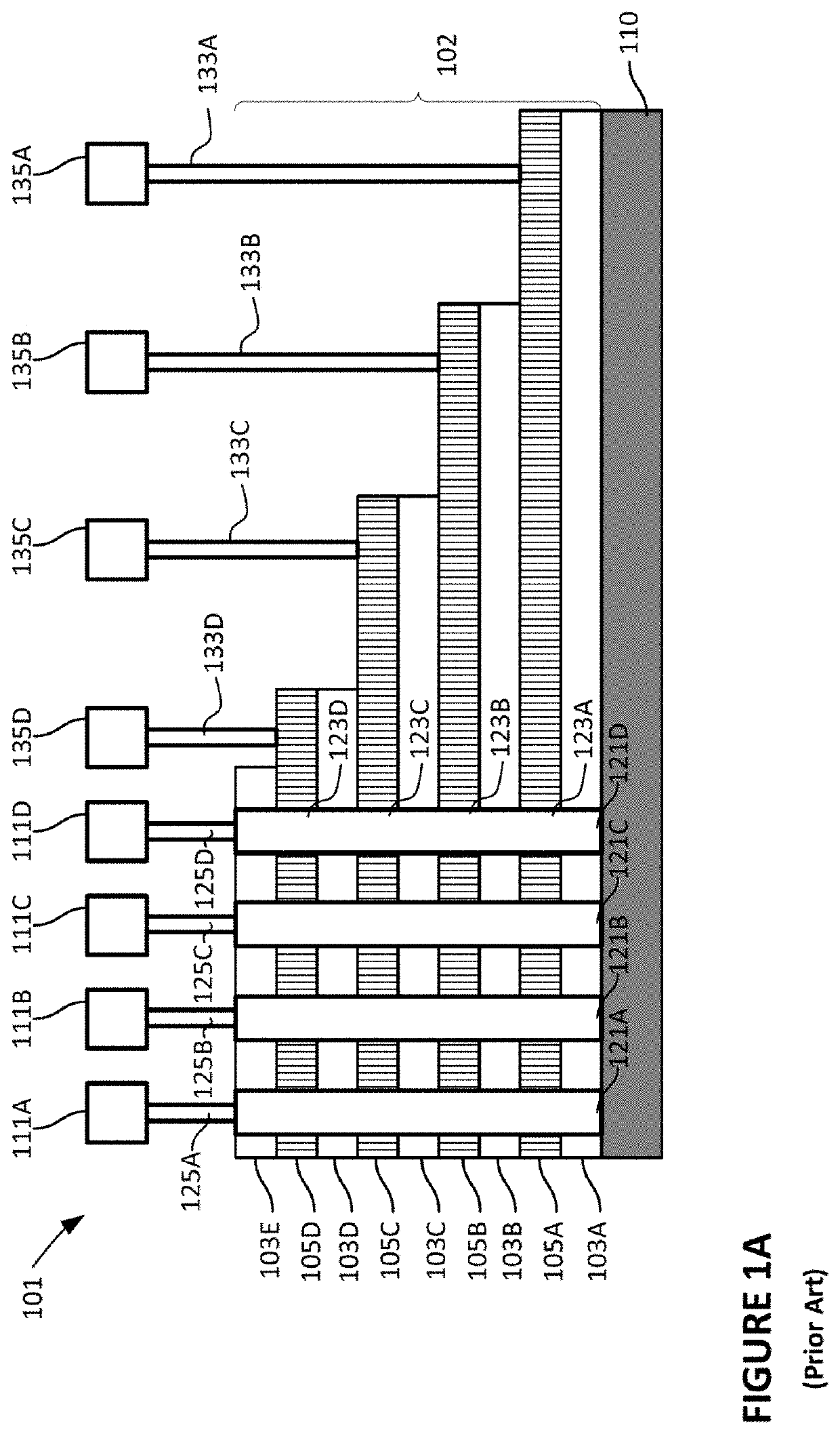
[0038]While the following disclosure provides a number of examples, it should be understood that the concepts and techniques are not limited to specific examples, but rather can be more broadly applied. For example, while the examples herein may refer to NAND memory, it should be understood that the technology described in such examples could also be applied to other devices, such as universal flash storage (UFS), solid state memory, Dynamic Random access memory (DRAM) or other such volatile or non-volatile memory.

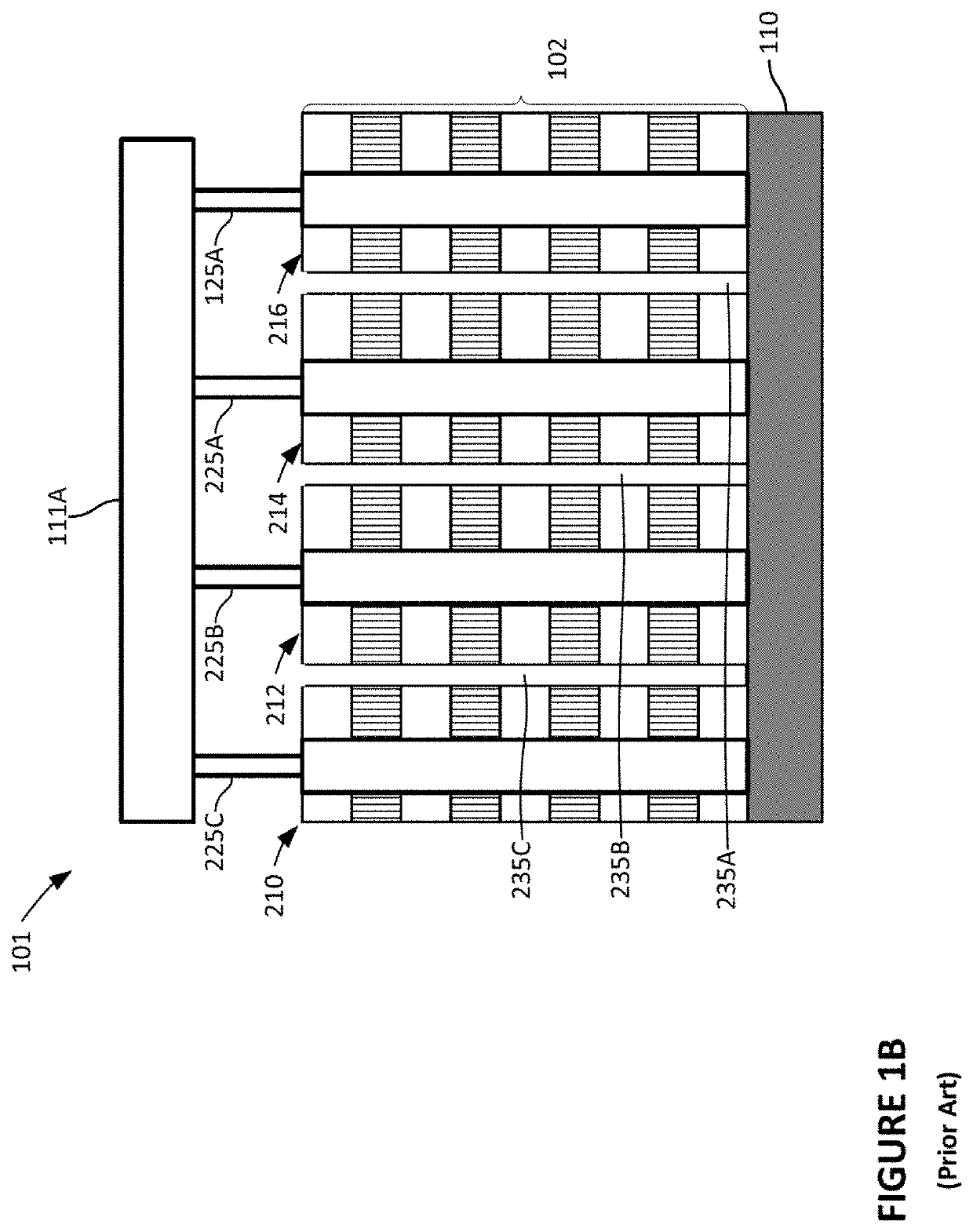
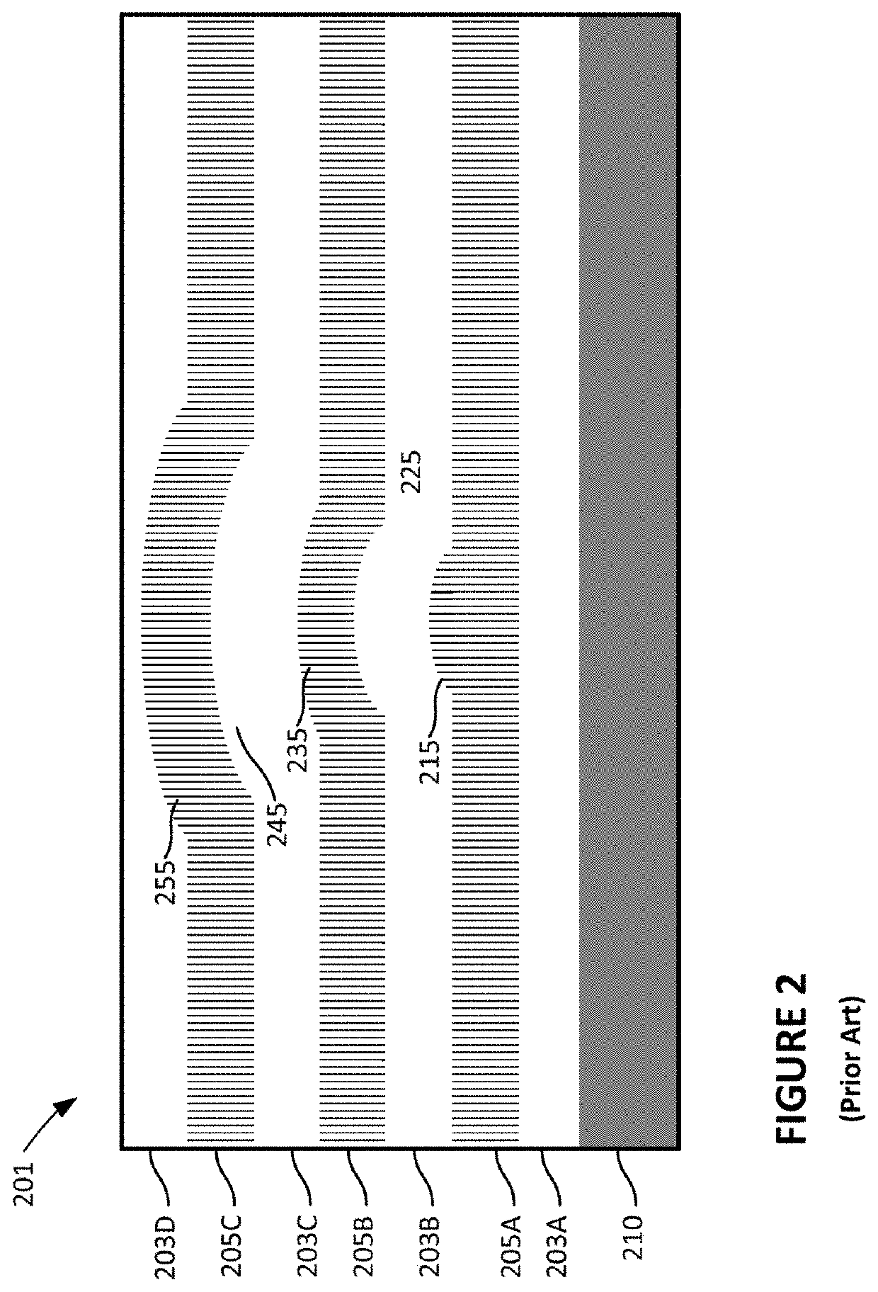
[0039]As used herein, 3D NAND memory, which may also be called vertical NAND (V-NAND), may include two-dimensional arrays of memory cells, typically found in planar NAND (“2D NAND”), stacked in vertical layers on a die to form memory cell stacks, referred to as memory pyramids in three-dimensions. Although the term memory pyramid is used to describe the memory cell stacks, the memory cell stacks may be in other shapes, such as a staircase type shape, box shape, etc.

[0040]M...


PUM


Abstract

Aspects of the disclosure relate to forming a completed stack of layers. Forming the completed stack of layers may include forming a first stack of layers on a first substrate and forming a second stack of layers on a second substrate. The first stack of layers may be bonded to the second stack of layers. The first or second substrate may be removed. Prior to bonding the first stack of layers and the second stack of layer, one or more holes may be etched in the first stack of layers. After removing the second substrate, one or more holes may be etched in the second stack of layers, wherein each of the one or more holes in the second stack of layers extend into a corresponding hole in the one or more holes in the first stack of layers.

Description

CROSS-REFERENCE TO RELATED APPLICATION[0001]The present application claims the benefit of the filing date of U.S. Provisional Patent Application No. 62 / 784,424 filed Dec. 22, 2018, the disclosure of which is hereby incorporated herein by reference.BACKGROUND[0002]NAND memory is a non-volatile storage technology. NAND memory provides large storage capacity with quick access times and low power usage within a robust package, making it commonplace in many modern electronic devices, such as solid-state hard drives, smart phones, flash drives, memory cards, computers, etc. The density of NAND memory, which is the number of memory cells found on a single die, defines the storage capacity for NAND memory.[0003]To increase the density of NAND memory, three-dimensional (3D) NAND was developed. FIG. 1A shows a side, cutaway view of a 3D NAND memory 101. The 3D NAND memory 101 includes memory pyramid 102. Memory pyramid 102 includes alternating and uniform layers of silicon oxide 103A-103E and...

Claims


Application Information

Patent Timeline
IPC IPC(8): H01L27/11582H01L27/11524H01L27/11556H01L27/1157
CPCH01L27/11582H01L27/1157H01L27/11556H01L27/11524H10B43/35H10B43/27H01L27/0688H01L21/6835H01L2221/6835H01L2221/68359H10B41/27H10B41/35
Inventor KATKAR, RAJESHCHANG, XUHABA, BELGACEM
Owner XCELSIS CORP
Features
  • Generate Ideas
  • Intellectual Property
  • Life Sciences
  • Materials
  • Tech Scout
  • Unparalleled Data Quality
  • Higher Quality Content
  • 60% Fewer Hallucinations
Learn More