Optical modulator

a modulator and optical technology, applied in non-linear optics, instruments, optics, etc., can solve the problems of preventing operation at high frequencies, limiting the high-speed modulation field, and a long length of about 10 cm, and achieve satisfactory high-frequency characteristics, low voltage, and low electrode loss

Active Publication Date: 2020-07-09
TDK CORPARATION
View PDF0 Cites 2 Cited by
  • Summary
  • Abstract
  • Description
  • Claims
  • Application Information

AI Technical Summary

Benefits of technology

[0026]According to the present invention, there can be provided a dual drive type optical modulator having low electrode loss, having satisfactory high-frequency characteristics, and capable of being driven with a low voltage due to improvement in efficiency of the electric field to be applied to the optical waveguide.

Problems solved by technology

The direct modulation system does not require the optical modulator and is thus low in cost, but has a limitation in terms of high-speed modulation and, thus, the external modulation system is used for high-speed and long-distance applications.
Although high-speed optical modulators having a modulation speed of 40 Gb / s or higher are commercially available, they have a major drawback that the entire length thereof is as long as about 10 cm.
However, the area of the ground electrode 24b is small, preventing operation at high frequencies.

Method used


Image

  • Optical modulator
  • Optical modulator
  • Optical modulator

Examples


examples

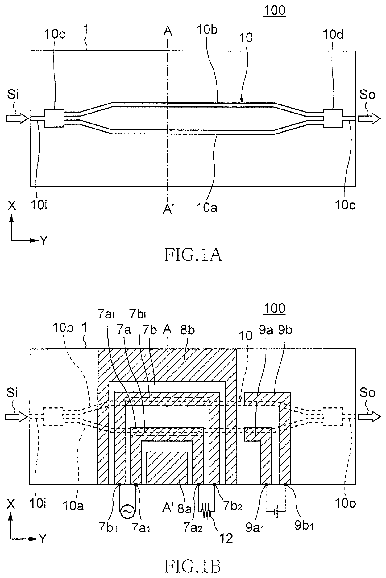
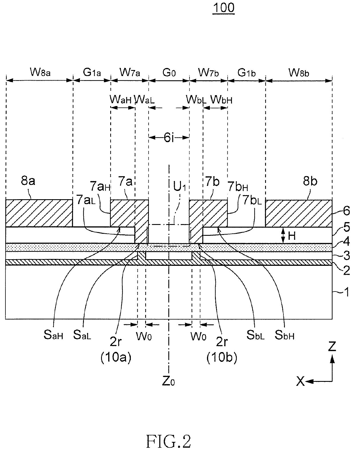
[0094]Electric field efficiency of an optical modulator having a cross-sectional structure illustrated in FIG. 2 was evaluated by simulation. In this optical modulator, the substrate 1 was a sapphire single crystal substrate (specific dielectric constant: 10), the waveguide layer 2 was formed of a lithium niobate film, the protective layer 3 was formed of SiO2 (specific dielectric constant: 4), the buffer layer 4 was formed of an oxide La-AL-O composed of, e.g., La and Al (specific dielectric constant: 13), the insulating layer 5 was formed of SiO2 (specific dielectric constant: 4), and the electrode layer was made of Au. The thickness of the waveguide layer 2 was 1.5 μm, the slab thickness of the waveguide layer 2 was 0.4 μm (the thickness of the ridge part 2r was 1.1 μm), the ridge width W0 of the waveguide layer 2 was 1.2 μm, the thickness of the buffer layer 4 was 0.9 μm, the gap between the first and second waveguides was 14 μm, the thickness H of the insulating layer 5 was 2 μ...


PUM

PropertyMeasurementUnit
lengthaaaaaaaaaa
thicknessaaaaaaaaaa
ridge width W0aaaaaaaaaa

Abstract

An optical modulator includes: first and second optical waveguides formed of an electro-optic material film on a substrate so as to have a ridge shape and to be disposed adjacent to each other; a buffer layer covering at least the upper surfaces of the first and second optical waveguides; and first and second signal electrodes provided above the buffer layer. The first and second signal electrodes have, respectively, first and second lower layer parts opposite, respectively, to the first and second optical waveguides through the buffer layer; and first and second upper layer parts provided, respectively, above the first and second lower layer parts. Widths of the lower surfaces of the first and second lower layer parts are smaller than widths of the first and second upper layer parts.

Description

TECHNICAL FIELD[0001]The present invention relates to an optical modulator used in the fields of optical communication and optical measurement and, more particularly, to an electrode structure of a Mach-Zehnder optical modulator.BACKGROUND ART[0002]Communication traffic has been remarkably increased with widespread Internet use, and optical fiber communication is becoming significantly important. The optical fiber communication is a technology that converts an electric signal into an optical signal and transmits the optical signal through an optical fiber and has wide bandwidth, low loss, and resistance to noise.[0003]As a system for converting an electric signal into an optical signal, there are known a direct modulation system using a semiconductor laser and an external modulation system using an optical modulator. The direct modulation system does not require the optical modulator and is thus low in cost, but has a limitation in terms of high-speed modulation and, thus, the exter...

Claims


Application Information

Patent Timeline
Patent Type & Authority Applications(United States)
IPC IPC(8): G02F1/225G02F1/035G02F1/03
CPCG02F1/035G02F1/225G02F2201/50G02F2001/212G02F1/0316G02F2202/20G02F1/212
Inventor IWATSUKA, SHINJIENDO, MAKOTOSASAKI, KENJI
Owner TDK CORPARATION
Why Eureka
Try Eureka