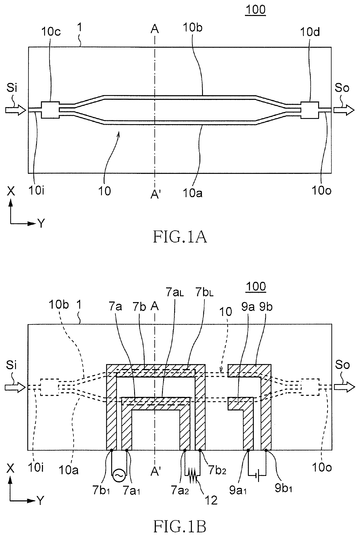
Optical modulator

a modulator and optical technology, applied in the field of optical modulators, can solve the problems of preventing operation at high frequencies, limiting the high-speed modulation field, and a large length of the entire length of the modulator, so as to reduce the eo characteristics of ripple or crosstalk, reduce radiation loss and wavelength chirp, and improve the effect of high-frequency characteristics

Active Publication Date: 2021-04-27
TDK CORPARATION +1
View PDF16 Cites 0 Cited by
  • Summary
  • Abstract
  • Description
  • Claims
  • Application Information

AI Technical Summary

Benefits of technology

[0012]An object of the present invention is therefore to provide a dual drive type optical modulator capable of improving velocity matching between signal wave and light, having a low electrode loss, having satisfactory high-frequency characteristics, and capable of being driven with a low voltage due to improvement in efficiency of an electric field to be applied to an optical waveguide.

Problems solved by technology

The direct modulation system does not require the optical modulator and is thus low in cost, but has a limitation in terms of high-speed modulation and, thus, the external modulation system is used for high-speed and long-distance applications.
Although high-speed optical modulators having a modulation speed of 40 Gb / s or higher are commercially available, they have a major drawback that the entire length thereof is as large as about 10 cm, which is disadvantageously long.
However, the area of the ground electrode 24b is small, preventing operation at high frequencies.
This is because, at high frequencies, current only flows in the vicinity of the electrode surface due to the skin effect to result in an increase in electrode loss.
However, increasing the thicknesses T of the signal electrodes 24a1 and 24a2 may reduce the effective dielectric constant of microwave to prevent velocity matching and may lower impedance to prevent impedance matching.
Further, increasing the widths W of the signal electrodes 24a1 and 24a2 may deteriorate efficiency of the electric field to be applied to the optical waveguide although the effective dielectric constant and impedance of microwave do not change significantly to result in an increase in half-wavelength voltage.
Therefore, in a conventional electrode structure, it is difficult to achieve a wider bandwidth of equal to or more than 35 GHz supporting high-speed transmission of 64 Gbaud.
Further, the effective dielectric constant of microwave depends on the dielectric constant of the buffer layer, so that it is difficult to match the velocity of microwave to the velocity of light by bringing the effective refractive index of microwave close to the effective refractive index of light.
When a ground electrode having a sufficient width or area cannot be provided in the vicinity of the signal electrode due to miniaturization or high integration of optical modulation device, ripple or crosstalk appearing in EO characteristics becomes a problem.
However, since the optical waveguide is very thin and narrow in line width, a problem of the electric field concentration is conspicuous.

Method used


Image

  • Optical modulator
  • Optical modulator
  • Optical modulator

Examples


examples

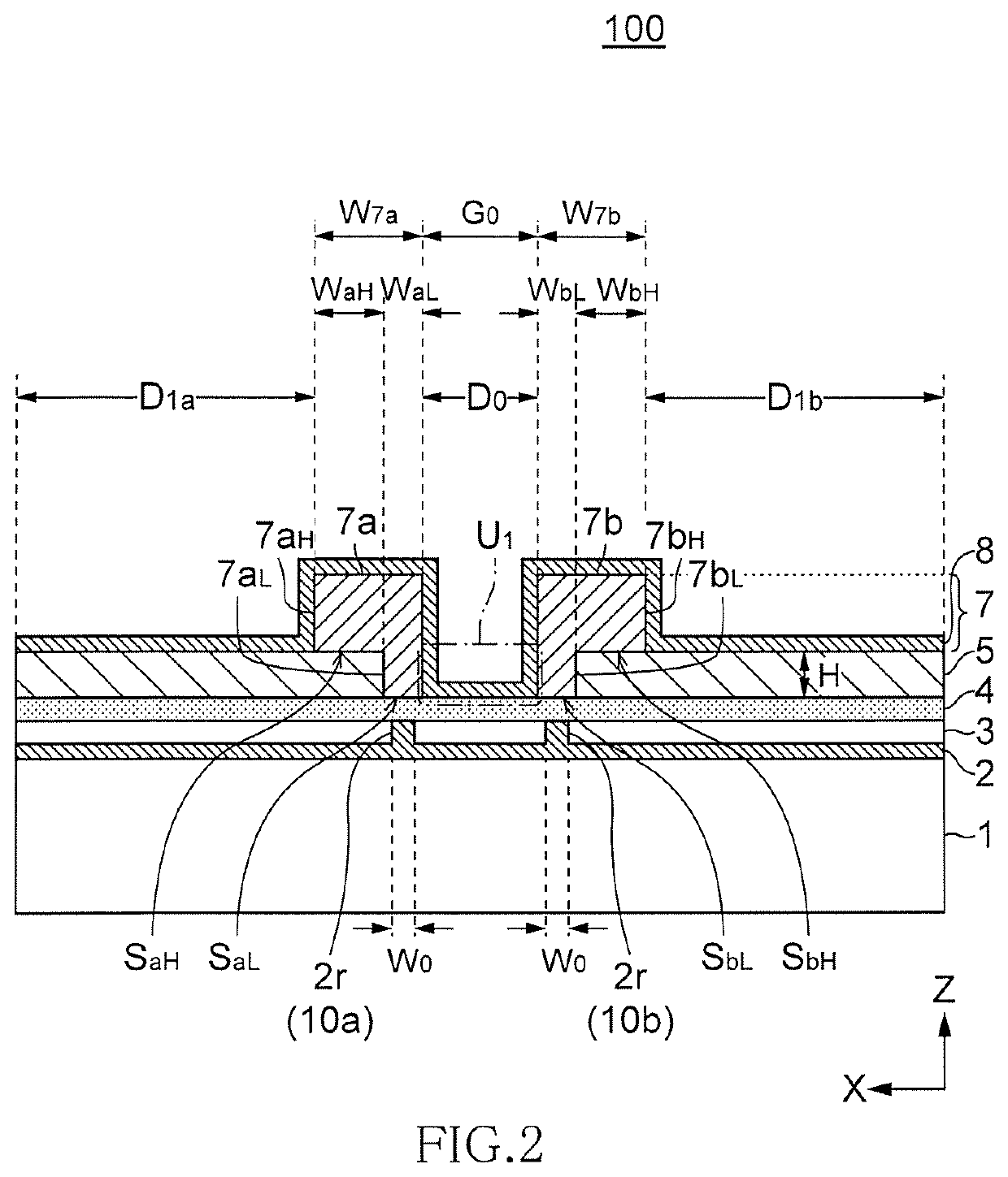
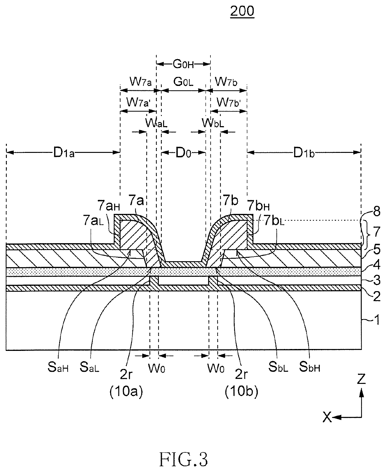
[0130]Electric field efficiency of an optical modulator having a cross-sectional structure illustrated in FIG. 2 was evaluated by simulation. In this optical modulator, the substrate 1 was a sapphire single crystal substrate (specific dielectric constant: 10), the waveguide layer 2 was formed of a lithium niobate film, the protective layer 3 was formed of SiO2 (specific dielectric constant: 4), the buffer layer was formed of an oxide La-AL-O (specific dielectric constant: 13) composed of La, Al and the like, the insulating layer 5 was formed of an oxide (specific dielectric constant: 8), the electrode layer 7 was made of Au, and the dielectric layer 8 was formed of polyimide. The thickness of the waveguide layer 2 was 1.5 μm, the slab thickness of the waveguide layer 2 was 0.4 μm (the thickness of the ridge part 2r was 1.1 μm), the ridge width W0 of the waveguide layer 2 was 1.2 μm, the thickness of the buffer layer was 0.9 μm, the gap between the first and second waveguides was 18 ...


PUM

PropertyMeasurementUnit
lengthaaaaaaaaaa
ridge width W0aaaaaaaaaa
thicknessaaaaaaaaaa

Abstract

An optical modulator is provided with a substrate, first and second optical waveguides each formed of a ridge-shaped electro-optic material film and disposed so as to be mutually adjacent on the substrate, a buffer layer covering upper surfaces of the first and second optical waveguides, first and second signal electrodes provided above the buffer layer so as to be opposed respectively to the first and second optical waveguides, and a dielectric layer covering at least one of a part of an exposed surface of the first signal electrode and a part of an exposed surface of the second signal electrode, and a part of an upper surface of the buffer layer. Differential signals are applied to the first and second signal electrodes.

Description

BACKGROUND OF THE INVENTIONField of the Invention[0001]The present invention relates to an optical modulator used in the fields of optical communication and optical measurement and, more particularly, to an electrode structure of a Mach-Zehnder optical modulator.Description of Related Art[0002]Communication traffic has been remarkably increased with widespread Internet use, and optical fiber communication is increasingly significant. The optical fiber communication is a technology that converts an electric signal into an optical signal and transmits the optical signal through an optical fiber and has a wide bandwidth, a low loss, and high resistance to noise.[0003]As a system for converting an electric signal into an optical signal, there are known a direct modulation system using a semiconductor laser and an external modulation system using an optical modulator. The direct modulation system does not require the optical modulator and is thus low in cost, but has a limitation in term...

Claims


Application Information

Patent Timeline
Patent Type & Authority Patents(United States)
IPC IPC(8): G02F1/225G02F1/03G02F1/21
CPCG02F1/2255G02F1/0316G02F2001/212G02F2201/063G02F2201/07G02F2201/127G02F2202/20G02F1/212
Inventor IWATSUKA, SHINJIENDOU, KENJIHARA, HIROKIMATSUURA, TOSHINORIKIKUKAWA, TAKASHIOHMORI, YASUHIRODOI, MASAHARUTAKEUCHI, SHINTAROTANAKA, TAKEHITOKUBOTA, YOSHINOBU
Owner TDK CORPARATION
Why Eureka
Try Eureka